Showing posts with label semiconductor. Show all posts

Apr 8, 2024

[Symposium] SFRC AIST

Advanced Semiconductor Research Center (SFRC) 
National Institute of Advanced Industrial Science and Technology (AIST)
1st Open Symposium 
https://unit.aist.go.jp/sfrc/sfrcsympo202405.html

Date: May 27, 2024
Venue: Fujisoft Akiba Plaza Akiba Hall (3 Kanda-Neribaki-cho, Chiyoda-ku, Tokyo) 
Hybrid event (on-site participation and remote streaming)

AGENDA:
Moderator: Takashi Matsukawa (Deputy Director, SFRC)
13:00-13:05 Opening Remarks Tetsuji Yasuda (AIST Electronics & Manufacturing)
13:05-13:10 Guest Greetings Mr. Tsutomu Kanashi (Director, Information Industry Division, Commerce and Information Policy Bureau, Ministry of Economy, Trade and Industry)
13:10-13:40 Keynote Speech 1 "Rapidus and Advanced Semiconductor Development" Masaharu Kobayashi (Rapidus Corporation)
13:40-14:10 Keynote Speech 2 "The Current Situation and Future of the Semiconductor Industry from a Systems Perspective" Kenji Tsuda (International Technology Journalist)
14:10-14:20 "Introduction to the Advanced Semiconductor Research Center" Akiue Masahara (Director, SFRC Research Center)
14:20-14:40 "Introduction of SCR Open Pilot Line" Fuminori Ito (Deputy Director, SFRC)
14:40-14:55 "2nm Generation GAA-FET Fundamental Technology" Hisashi Irizawa (SFRC) Head, Device Process Research Team)
14:55-15:10 "Extreme Device and Material Technology for the 2nm Generation and Beyond" Naoya Okada (Head, Extreme CMOS Materials Research Team, SFRC)
15:10-15:30 Coffee Break
15:30-16:00 Keynote Speech 3 "What is Open Source Utilized Silicon Initiatives (Open-SUSI)?" Jun-Ichi Okamura (AIST Solutions)
16:00-16:15 "Device Integration Technology by 3D Integrated Packaging Technology Katsuya Kikuchi (Director, SFRC 3D Integrated Technology Research Team)
16:15-16:30 "Advanced System-on-Chip (SoC) Design Technology"
Shinichi Ouchi (AIDL Laboratory Team Leader/SFRC Integrated Circuit Design Research Team)
16:30-16:45 Environmental Impact Assessment of Semiconductor Manufacturing and Greening Technologies" Shinji Mimida (SFRC)
16:45-17:00 "Quantum-related semiconductor integrated device technology" Takahiro Mori (Director, SFRC New Principles Silicon Device Research Team)
17:00-17:15 Q&A
17:15-17:30 Closing Remarks Takashi Nakano (Deputy Director, Research Strategy Planning Department, AIST)

On-site participation, remote participation: Participation is free. (Please register for this form) Remote streaming is scheduled for Zoom. Please register one by one if you wish to participate. Please note that there is a limit to the number of participants at the venue.

Secretariat contact <https://unit.aist.go.jp/sfrc/sfrcsympo202405.html>
National Institute of Advanced Industrial Science and Technology (AIST) Advanced Semiconductor Research Center Symposium Secretariat (M-SFRC-Sympo-ml@aist.go.jp)

Nov 21, 2023

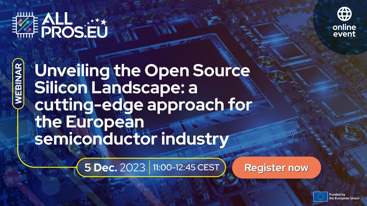
[webinar] Open Source Silicon Landscape

Unveiling the Open Source Silicon Landscape
a cutting-edge approach for the European semiconductor industry
5 December 2023


Who should attend and why:
  • Policymakers at the regional, national, and European level who want to strengthen their respective semiconductor ecosystem while collaborating and contributing to the Union’s industry as a whole
  • Research and academia representatives who are interested in deepening their knowledge or discovering the potential of the Open Source Silicon landscape
  • SMEs in the semiconductor industry who aim to expand and innovate their business by using a cutting-edge approach
  • Start-ups that are eager to elevate their business to the next level by embracing vanguard strategies
  • Citizen scientists and the general public who would like to have a better understanding of the new horizons in the semiconductor landscape
  • Experts active in industrial development who are interested in integrating potential new approaches
Registration:

The event is free of charge, but registration is mandatory. Registrants will receive the link to access the event by email.

Agenda:

11:00 - 11:05 Welcome
11:05 - 11:10 Introducing Open Source Silicon
11:10 - 11:20 BACKGROUND Open source silicon between software and hardware Background
11:20 - 11:40 POLICY BRIEF PRESENTATION Open source silicon’s position in the semiconductor value chain
11:40 - 12:35 PANEL Key opportunities and threats relevant to open source silicon strategies
12:35 - 12:45 Q&A and conclusions

Oct 30, 2023

[paper] DEVSIM

Sanchez, J. E.,
DEVSIM: A TCAD Semiconductor Device Simulator
Journal of Open Source Software, 7(70), 3898, (2022).
DOI:10.21105/joss.03898

Abstract: DEVSIM is technology computer-aided design (TCAD) software for semiconductor device simulation. By solving the equations for electric fields and current flow, it simulates the electrical behavior of semiconductor devices, such as transistors. It can be used to model existing, fabricated devices for calibration purposes. It is also possible to explore novel device structures and exotic materials, reducing the number of costly and time-consuming manufacturing iterations While DEVSIM has limited capabilities for the creation of 1-D and 2-D meshes, the Pythoninterface allows the import of mesh structures from any format using a triangular representation (in 2-D) or a tetrahedral representation (in 3-D). This makes it possible for the user to utilize high quality open source meshing solutions.

FIG: 90-nm 3-D MOSFET. The polysilicon gate (2) is surrounded by oxide (5) and two nitride regions (3) and (4). The bulk region (1) has a 120nm drawn gate length. The source and drain contacts are both 50 nm underneath the nitride regions. A body contact was placed on the bottom of the 60nm silicon region. The oxide thickness is 4.9 nm and the device is 25nm thick.


Oct 13, 2023

[conference] FIRST 2023


Website: http://sme.tju.edu.cn/info/1095/2265.htm
English: https://www.aconf.org/conf_194081.html

Date: 30 Oct 2023 (Mon) to 31 Oct 2023 (Tue)
Main Organizer: Tianjin University
Venue: Online

Theme: Interdisciplinarity: The Fusion of Technologies (Semiconductor, Artificial Intelligence, Internet-of-Things, and Communications)

The inaugural FIRST international conference will be held online on Monday, 30th and Tuesday 31st October 2023. Many world-renowned professors, experts and researchers in communication and semiconductor technologies and other related fields at home and abroad will attend this conference. This international conference aims to discuss the open problems and present new solutions that address the challenges of future communication systems, artificial intelligence, internet-of-things, and chip design. Specifically, the role of semiconductors in future communications will be presented and how can the semiconductor and communication industry emerge stronger after the pandemic will be discussed.

This FIRST international conference will be open to relevant enterprises and experts in the field of semiconductors and integrated circuits, providing a professional multi-disciplinary and multi-field exchange and cooperation platform for enterprises, universities and research institutes in the field of semiconductors and integrated circuits, providing innovative ideas for today's increasingly complex and difficult product development, combining cutting-edge scientific research and product innovation more effectively. At the same time, it lays a solid foundation for more in-depth school-enterprise cooperation.

Registration(注册网址): 中文站 - https://www.aconf.cn/conf_194081.html


Sep 10, 2023

[book] Advanced Ultra Low-Power Semiconductor Devices

Advanced Ultra Low-Power Semiconductor Devices
Design and Applications

Edited by Shubham Tayal, Abhishek Kumar Upadhyay, Shiromani Balmukund Rahi, and Young Suh Song

ISBN: 9781394166411 | (C)2023  Hardcover | 306 pages

Description
This outstanding new volume offers a comprehensive overview of cutting-edge semiconductor components tailored for ultra-low power applications. These components, pivotal to the foundation of electronic devices, play a central role in shaping the landscape of electronics. With a focus on emerging low-power electronic devices and their application across domains like wireless communication, biosensing, and circuits, this book presents an invaluable resource for understanding this dynamic field.

Bringing together experts and researchers from various facets of the VLSI domain, the book addresses the challenges posed by advanced low-power devices. This collaborative effort aims to propel engineering innovations and refine the practical implementation of these technologies. Specific chapters delve into intricate topics such as Tunnel FET, negative capacitance FET device circuits, and advanced FETs tailored for diverse circuit applications.

Beyond device-centric discussions, the book delves into the design intricacies of low-power memory systems, the fascinating realm of neuromorphic computing, and the pivotal issue of thermal reliability. Authors provide a robust foundation in device physics and circuitry while also exploring novel materials and architectures like transistors built on pioneering channel/dielectric materials. This exploration is driven by the need to achieve both minimal power consumption and ultra-fast switching speeds, meeting the relentless demands of the semiconductor industry. The books scope encompasses concepts like MOSFET, FinFET, GAA MOSFET, the 5-nm and 7-nm technology nodes, NCFET, ferroelectric materials, subthreshold swing, high-k materials, as well as advanced and emerging materials pivotal for the semiconductor industrys future.

Aug 2, 2023

[video] Semiconductor industry in Switzerland

75th Anniversary of the Transistor
Semiconductor Industry in Switzerland

A commemorative and networking event was organized by the IEEE Solid-State Circuits Chapter of Switzerland at the EPFL Microcity building in Neuchâtel, Switzerland. In the first part of the afternoon, we had the honor to host three Distinguished Lecturers:
  • Prof. Tom Lee presentation “From Rocks to Chips: Stories of the Transistor” covered the early history of the transistor.
  • Dr. Chris Mangelsdorf described circuit design techniques using the bipolar junction transistor (BJT) in his talk “Don’t Try This With CMOS!”.
  • Prof. Christian Enz concluded this session, describing the development of low power CMOS using the EKV MOSFET model.
This video covers the second part of the event, “From transistor manufacturing in the late 1950’s until today”. It hosted five speakers who were key actors or are still active in the semiconductor sector of Switzerland.


Jun 27, 2023

[paper] Logic Without CMOS

Jonathan Hall and Manus Hayne
Logic Without CMOS: A III-V Semiconductor, Single Charge Carrier Approach to Digital Logic
WOCSDICE-EXMATEC 2023, Palermo (Italy), 21-25 May 2023

Department of Physics, Lancaster University, Lancaster, United Kingdom

Abstract: A new patent-pending approach to digital logic devices is proposed as an alternative to complimentary metal-oxide-semiconductor (CMOS) logic. A novel III-V semiconductor digital logic device combines both the “n” and “p” equivalents of CMOS into a single heterostructure device using just one type of charge carrier. The device, which forms an inverter, consists of two charge-accepting channel layers which sandwich a central electron (or hole) reservoir. Under zero bias the charge remains in the reservoir with both channel layers absent of free charge carriers (off state). Once a bias is applied to the gate, charge is either pushed into the bottom channel (negative bias) or pulled into the top channel (positive bias) turning one channel on whilst the other remains off. Thus, the complementary behaviour of logic, in which one part of the logic element is on and the other is off, is achieved without the asymmetry of hole and electron mobility. Proof of concept devices have been designed in both the well documented GaAs/AlxGa1-xAs system and in the 6.1Å family of semiconductors. One-dimensional, room temperature energy-band simulations using nextnano++ (software for semiconductor devices) [1] have shown effective and symmetric logic function at low voltage and an excess of 1,000× charge density ratio between the two channels under operation. Proof of concept devices are currently undergoing fabrication.

Fig: Proposed device architecture for an inverter, utilising electrons as the charge carrier. The “N” and “P” charge-accepting layers represent the equivalent CMOS transistors. With positive VG, the electrons are pulled from the reservoir into the upper channel, and with negative VG, the electrons are pushed into the lower channel. With zero bias, the charge remains within the reservoir and the channels are resistive (off). The barrier layers can consist of grown semiconductor or deposited dielectric.

Acknowledgments: Thanks to the Leverhulme Trust for a PhD studentship for Jonathan Hall and to nextnano for access to their software.


Jun 14, 2023

[review] TCAD Simulations of Semiconductor Piezoresistance

Takaya Sugiura, Kazunori Matsuda*, Nobuhiko Nakano
Review: Numerical Simulations of Semiconductor Piezoresistance for Computer-Aided Designs
in IEEE J-EDS, vol. 11, pp. 325-336, 2023
DOI: 10.1109/JEDS.2023.3281866

  Department of Electronics and Electrical Engineering, Keio University, Yokohama, Kanagawa, Japan
* Division of Electrical, Electronic and Infocommunications Engineering, Osaka University, Suita, Japan

Abstract: The field of piezoresistance has mainly advanced through experimental research; however, the improved accuracy of simulations and the emergence of new materials have increased the importance of simulations in this field. This review discusses the methods and current topics related to simulations of piezoresistive devices. Advancing simulation modeling will facilitate the computer-aided design of piezoresistive devices, and this review introduces the means of establishing these models by discussing the current studies on simulations and calculations in this field. Two simulation methods currently exist namely, device simulations and first-principles theoretical analysis. This review focuses on numerical simulation approaches for modeling of the piezoresistive effect using the multiphysics simulations of the mechanical and electrical behaviors of piezoresistive materials.

FIG: Basic simulation flow for studies on semiconductor piezoresistors.

Feb 9, 2023

[Hisayo Momose] My Journey as a Researcher in the Semiconductor Field

graphical user interface, text, application 

Hisayo Mosmose's Story 

Read Hisayo Momose's article from the IEEE EDS January Newsletter, "My Journey as a Researcher in the Semiconductor Field."

Dr. Momose has more than 30 years of experience in research and development at Toshiba Corporation, Japan. She is a recipient of several awards and honors, and has authored or co-authored nearly 200 papers published in technical journals and conference proceedings [read more...]

#IEEE #EDS #ElectronDevices #WiEDS #womeinengineering #semiconductors


Jan 30, 2023

[paper] DMT-core: A Python Toolkit for Semiconductor Device Engineers

Mario Krattenmacher1,2, Markus Müller1,2, Pascal Kuthe1,2, and Michael Schröter1,2
DMT-core: A Python Toolkit for Semiconductor Device Engineers
Journal of Open Source Software, 7(75), 4298
DOI: 10.21105/joss.04298
1 CEDIC, TU Dresden, Dresden (D)
2 SemiMod GmbH, Dresden (D)

Abstract: Semiconductor device engineers are faced by a number of non-trivial tasks that can be solved efficiently using software. These tasks include, amongst others, data analysis, visualization and processing, as well as interfacing various circuit and Technology-Computer-Aided-Design (TCAD) simulators. In practice, custom ‘home-made’ scripts of varying quality are employed to solve these tasks. It is often found that fundamental software engineering concepts, such as Test-Driven-Development (Shull et al., 2010), or the use of state-of-the-art version control tools (e.g. Git) and practices (e.g. continuous integration, CI), are not utilized by these scripts. The issues inflicted by this practice include:
  • The analysis/visualization/generation of data becomes difficult to reproduce.
  • Device engineers work far from their maximum work-efficiency, as they are hindered, instead of empowered, by the software infrastructure.
  • Knowledge built-up, possibly over decades, may be lost when developers leave a company or institution.
The Device Modeling Toolkit (DMT) presented here aims to solve these issues. DMT provides a Python library that offers:
  • classes and methods relevant to commonly used device engineering tasks
  • several abstract base classes for implementing new interfaces to various types of simulators
  • concrete implementations of the abstract base classes for open-source simulators such as Ngspice (Vogt, 2022), Xyce (Keiter et al., 2014) or Hdev (Müller et al., 2022).
DMT-based simulations allow data generation, workflow implementation and visualization to be implemented in a single file, enabling more efficient cooperation and more reproducible research (Stodden et al., 2016). Basic principles in software engineering, such as unit testing,v ersion control, and documentation, are adhered to so that others can use and contribute to the software.
FIG: DMT interfacing a circuit simulator and corresponding data flow.

Related Publications: DMT is used internally by CEDIC staff in research and by SemiMod for commercial purposes. It has also been used by cooperating institutions and companies. The project has been used inthe following contexts:
  • for circuit simulations (Weimer et al., 2022),
  • for TCAD simulations and plotting (Markus Muller et al., 2021),
  • for circuit and TCAD simulations (M. Muller et al., 2022),
  • for model parameter extraction (Müller & Schröter, 2019) and
  • for model parameter extraction and TCAD simulation (Phillips et al., 2022).
In addition, DMT has been cited in (Grabinski, 2019; Kuthe et al., 2020; Müller et al., 2019,
2021).

Related Projects: DMT directly uses the VerilogAE (Kuthe et al., 2020) for accessing all information in Verilog-AMS files. The TCAD simulator Hdev (Müller et al., 2022) uses the class DutHdev as its Python interface.

Acknowledgements: This project would not have been possible without our colleagues Dipl.-Ing. Christoph Weimer and Dr.-Ing. Yves Zimmermann. We particularly acknowledge Wladek Grabinski for his efforts to promote the use of open source software in the semiconductor community.

REF:
Shull, F., Melnik, G., Turhan, B., Layman, L., Diep, M., & Erdogmus, H. (2010). What do we know about test-driven development? IEEE Softw., 27(6), 16–19. https://doi.org/10.1109/MS.2010.152
Vogt, H. (2022). Ngspice, the open source Spice circuit simulator - Intro. http://ngspice. sourceforge.net/
Keiter, E. R., Mei, T., Russo, T. V., Schiek, R. L., Sholander, P. E., Thornquist, H. K., Verley, J. C., & Baur, D. G. (2014). Xyce Parallel Electronic Simulator Reference Guide , Version 6 . 2 (September). Sandia National Laboratories (SNL). https://doi.org/10.2172/1826862
Müller, M., Mothes, S., Claus, M., & Schröter, M. (2022). Hdev: A 1D and 2D Hydrodynamic/Drift-Diffusion solver for SiGe and III-V HBTs. J. Open Source Software
Stodden, V., McNutt, M., Bailey, D. H., Deelman, E., Gil, Y., Hanson, B., Heroux, M. A., Ioannidis, J. P. A., & Taufer, M. (2016). Enhancing reproducibility for computational methods. Science, 354(6317), 1240–1241. https://doi.org/10.1126/science.aah6168 
Grabinski, W. (2019). FOSS TCAD/EDA tools for compact modeling. Arbeitskreis Bipolar.
https://www.iee.et.tu-dresden.de/iee/eb/forsch/AK-Bipo/2019/7-MOS-AK-Association_wgr_BipAK19.pdf


Sep 14, 2022

Future Horizons Semiconductor Industry Update Webinar

Has the chip market boom come to an end? What fate now awaits the industry? Find out the answer to these and other key questions at Future Horizons' IFS2022 Mid-Term Semiconductor Industry Update Webinar, Sep 13, 2022 - 3pm UK BST (GMT+1):
https://www.futurehorizons.com/page/136/Industry-Update-Webinar


Why? Founded in 1989, Future Horizons’ track record and industry experience makes this a must-attend event for key decision makers in the semiconductor, electronics and all related industries. We always present accurate and insightful analysis at these events backed up by sound data

What You Will Learn: This one-hour broadcast will focus on the chip industry outlook, including:
• Has the market boom turned to bust
• What is the market outlook for 2023
• What are the exposures, vulnerabilities, opportunities, losers and gainers
• What will the likely downturn repercussions be
• How to build resilient strategies and business models
• Opportunity to ask specific questions in advance, during and after the webinar.

Who Should Attend?
• All companies, small and large, from startups to established market leaders
• Key decision-makers engaged in the design, manufacture, or supply of semiconductors
• Government organisations involved in trade and investment
• Those involved in investing or banking within the electronics industry
• Senior marketing executives planning future marketing strategy

Why Future Horizons?
We have been in the business of forecasting and analysing the semiconductor market for over 55 years and have been a trusted advisor to governments, investors and most of the top global semiconductor firms. Time and time again, we have delivered sound advice and saved our clients time and money with our forensic and accurate analysis of the industry.

Malcolm Penn; Chairman & CEO; Future Horizons Registered Company: 4380991

Future Horizons on Social Media
Follow FH on Twitter, like FH on Facebook and join FH Linked In Group and receive regular industry news, information and comments.


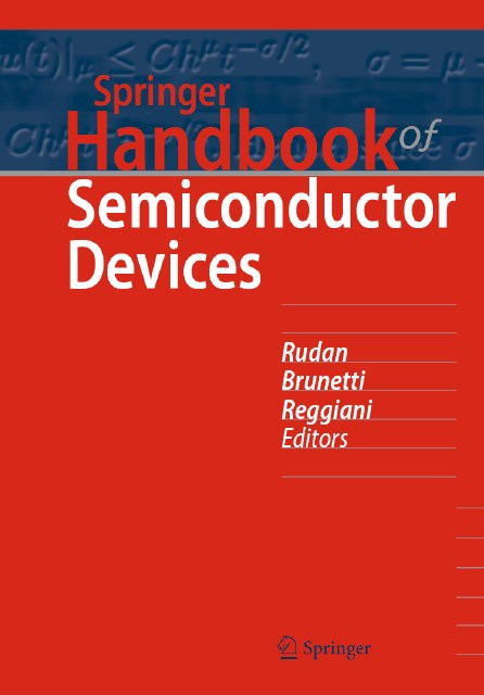
Handbook of Semiconductor Devices

Massimo Rudan, Rossella Brunetti, Susanna Reggiani (Eds.)
Springer Handbook of Semiconductor Devices
Series: Springer Handbooks
1st ed., 2022, ca. 1700 p., 1300 illus.

Order online at link.springer.com or customerservice@springernature.com
  • Covers physical backgrounds, fabrication, application and modeling
  • Describes in detail both conventional and innovative devices
  • An indispensable resource for practitioners, professionals and researchers


This Springer Handbook comprehensively covers the topic of semiconductor devices, embracing all aspects from theoretical background to fabrication, modeling, and applications.

Nearly 100 leading scientists from industry and academia were selected to write the handbook's chapters, which were conceived for professionals and practitioners, material scientists, physicists and electrical engineers working at universities, industrial R&D, and manufacturers.

Starting from the description of the relevant technological aspects and fabrication steps, the handbook proceeds with section fully devoted to the main conventional semiconductor devices like, e.g., bipolar transistors and MOS capacitors and transistors, used in the production of the standard integrated circuits, and the corresponding physical models. In the subsequent chapters, the scaling issues of the semiconductor-device technology are addressed, followed by the description of novel concept-based semiconductor devices. The last section illustrates the numerical simulation methods ranging from the fabrication processes to the device performances.

Each chapter is self-contained, and refers to related topics treated in other chapters when necessary, so that the reader interested in. specific subject can easily identify personal reading path through the vast contents of the handbook.

Technological aspects
CMOS Manufacturing processes. Semiconductor memory technologies. BCD process technologies. Measuring techniques for the semiconductor's parameters. Interconnect Processing: Integration, Dielectrics, Metals. Wet Chemical Processes for BEOL Technology. From FinFET to nanosheets and beyond. Advanced Lithography. Advanced technologies for future materials and devices

Basic devices and applications
MOS Capacitors, MOS Transistors and Charge-Transfer Devices. Electrostatic doping and devices. Planar MOSFETs and their application to IC design. Silicon power devices. Silicon Carbide Power Devices. GaN- based lateral and vertical devices. Bipolar transistors and silicon diodes. Memory Challenges. Silicon sensors. Solar Cells. X-ray detectors. Photodetectors based on Emerging Materials. Terahertz Electronic Devices. Semiconductor Lasers

New-generation devices and architectures
Heterojunction tunnel field-effect transistors. Carbon based field-effect transistors. Negative capacitors and applications. Flexible Electronics and Biomedical Sensors. Bio-Degradable Electronics. Resistive Switch- ing Memories. Phase-Change Memories. Spin-Based Devices for Digital Applications. Memristive/CMOS devices for neuromorphic applications. Nanoelectronic Systems for quantum computing

Modeling
Compact/SPICE Modeling. Process simulation. A digital twin for MEMS and NEMS. Macroscopic Transport Models for Classical Device Simulation. Grid generation and Algebraic solvers. Spherical Harmonics Expansion and Multi-Scale Modeling. Charge Transport Models for Amorphous Chalcogenides. Application of the k.p method to device simulation. Ab initio methods for electronic transport in semiconductors and nanostructures. Quantum Transport in the Phase Space, the Wigner Equation. The Non-Equilibrium Green Function (NEGF) Method. Tight-Binding Models, their Applications to Device Modeling and Deployment to. Global Community

Mar 18, 2022

[paper] Compound-Semiconductor Memory on Silicon

Peter D. Hodgson, Dominic Lane, Peter J. Carrington, Evangelia Delli,
Richard Beanland, and Manus Hayne
ULTRARAM: A Low-Energy, High-Endurance, 
Compound-Semiconductor Memory on Silicon 
Adv. Electron. Mater. 2022, 2101103
DOI: 10.1002/aelm.202101103
  
Department of Physics, University of Warwick (UK)


Abstract: ULTRARAM is a nonvolatile memory with the potential to achieve fast, ultralow-energy electron storage in a floating gate accessed through a triple-barrier resonant tunneling heterostructure. Here its implementation is reported on a Si substrate; a vital step toward cost-effective mass production. Sample growth using molecular beam epitaxy commences with deposition of an AlSb nucleation layer to seed the growth of a GaSb buffer layer, followed by the III–V memory epilayers. Fabricated single-cell memories show clear 0/1 logic-state contrast after ≤10 ms duration program/erase pulses of ≈2.5 V, a remarkably fast switching speed for 10 and 20 µm devices. Furthermore, the combination of low voltage and small device capacitance per unit area results in a switching energy that is orders of magnitude lower than dynamic random access memory and flash, for a given cell size. Extended testing of devices reveals retention in excess of 1000 years and degradation-free endurance of over 107 program/erase cycles, surpassing very recent results for similar devices on GaAs substrates.
Fig: ULTRARAM device concept. a) Schematic cross-section of a device with corresponding material layers. The floating gate (FG), triple-barrier resonant-tunneling structure (TBRT), and readout channel are highlighted. Arrows indicate the direction of electron flow during program/ erase operations. b) Scanning electron micrograph of a fabricated device of 10 µm gate length. 

Acknowledgements: P.D.H. and D.L. contributed equally to this work. This work was supported by the Engineering and Physical Sciences Research Council, UK, via the 2017–2020 Impact Acceleration Account funding allocation to Lancaster University under grant EP/R511560/1, a scholarship under grant EP/N509504/1, equipment funding under grant EP/T023260/1, and the Future Compound Semiconductor Manufacturing Hub grant EP/P006973/1, by the ATTRACT project funded by the EC under Grant Agreement 777222 and by the Joy Welch Educational Charitable Trust.

Aug 25, 2020

[paper] Native High-k Oxides for 2D Transistors

Yury Yu. Illarionov1,2, Theresia Knobloch1 and Tibor Grasser1
Native high-k oxides for 2D transistors
Nature Electronics vol. 3, pp 442–443 (2020)
Published online: 05 August 2020
DOI: 10.1038/s41928-020-0464-2

1Institute for Microelectronics, TU Wien, Vienna, Austria
2Ioffe Physical-Technical Institute, St Petersburg, Russia

Abstract: The two-dimensional semiconductor Bi2O2Se can be oxidized to create an atomically thin layer of Bi2SeO5 that can be used as the insulator in scaled field-effect transistors.

Fig.: Development of FETs with Bi2O2Se channels and native Bi2SeO5 insulators. a.) Step-by-step oxidation of multilayer Bi2O2Se towards Bi2SeO5 and the crystal structure of the two materials. b.) Cross-sectional scanning transmission electron microscopy image confirming the atomically sharp interface. c.) Schematic of the top-gated devices fabricated with a native gate oxide. d.) Gate transfer characteristics of the devices with a 4.6-nm-thick Bi2SeO5 layer (EOT below 1 nm)

Jul 29, 2020

Jerzy Ruzyllo - Guide to Semiconductor Engineering

Guide to Semiconductor Engineering
Jerzy Ruzyllo1 (Pennsylvania State University, USA)
World Scientific Book Series. March 2020
This Guide to Semiconductor Engineering is concerned with semiconductor materials, devices and process technologies which in combination are the driving force behind the unprecedented growth of our technical civilization over the last half a century. This book was conceived and written keeping in mind those who need to learn about semiconductor engineering, who are professionally associated with select aspects of this technical domain and want to see it in a broader context, or are simply interested in semiconductors. In its coverage of semiconductor engineering this Guide departs from textbook-style, monothematic in-depth coverage of topics such as the physics of semiconductors and semiconductor devices, the manufacturing of semiconductor devices and circuits, and the characterization of semiconductor materials. Instead, it covers the entire field of semiconductor engineering in one concise volume with synergistic interactions between various areas clearly identified. It is a holistic approach to the coverage of semiconductor engineering which makes this guide unique among books covering semiconductor related issues available on the market today. 
[Table of Contents]
1Jerzy Ruzyllo is a Distinguished Professor Emeritus in the School of Electrical Engineering and Computer Science at the Pennsylvania State University. He joined Penn State in 1984 after completing his education, obtaining a PhD degree in 1977, and serving on the faculty of the Warsaw University of Technology in Poland. Throughout his career, Dr Ruzyllo was actively involved in research and teaching in the area of semiconductor science and engineering. Dr Ruzyllo is a Life Fellow of IEEE and Fellow of the Electrochemical Society.

Oct 25, 2013

MIEL2014 Abstracts Deadline Extension

IEEE 29th International Conference on Microelectronics (MIEL 2014) is to be held on 11-14 May 2014 at the Serbian Academy of Science and Arts, Belgrade, Serbia. The extended submission deadline for 2-page extended abstracts of regular contributions had been set to 26th, but, due to many requests by authors, we will continue receiving the submissions by October 31st 2013.

More detailed information on MIEL 2014 can be found in the attached Call for Papers, as well as on the conference web site http://miel.elfak.ni.ac.rs/. We will be looking forward to receiving your submission and seeing you at our conference next year in May.

[read more...]

Jan 9, 2013

10th IWCM Workshop Program

10th International Workshop on Compact Modeling 

January 22 (Tue), 2013 

Pacifico Yokohama, Room 419

Yokohama, Japan

Time
#
Title
Authors
Affiliation
9:00-9:10

Opening: H. J.  Mattausch (Workshop Chair)


Power Devices   Chair: D. Navarro


9:10-9:30
1
HiSIM_HV Temperature Modeling for Multi-Geometry LDMOS: Comparison of the Temperature Flag Options
Y. Iino
Silvaco Japan
9:30-9:50
2
Analysis and Further Improvements of the Drain-Resistance Modeling in HiSIM_HV
T. Umeda et al.
Hiroshima University
9:50-10:10
3
Floating-Base Effect Modeling for IGBT Structure using Potential Modification
T. Yamamoto
et al.
Denso
10:10-10:30

- Break -


Novel FET Structures Chair: T. Nakagawa


10:30-10:50
4
Study on Dynamic Threshold Nanowire Tunnel FET
A. Zhang et al.
Peking University
Shenzhen
10:50-11:10
5
A DC Model of TFETs for SPICE Simulations
L. Zhang and M. Chan
HK UST 
11:10-11:30
6
A Surface Potential Based Compact Model of Organic Thin-Film Transistor for Circuit Simulation
T.K. Maiti et al.
Hiroshima University
11:30-11:40

-  Break -


Optical and Wireless Chair: J. He


11:40-12:00
7
An Embedded Modulation of Silicon Germanium FIN-LED - A simulation study
J. Kwon et al.
Seoul National
University
12:00-12:20
8
Predicting Key Parameters of Inductive Power Links
S. Raju et al.
HK UST 
12:20-14:00

- Lunch Break -


Aging and Degradation Chair: M. Miura-Mattausch


14:00-14:40
9
Invited Keynote: Interaction of Bloch Carrier and Bound State in the Reliability Modeling
Y.J. Park and
S. Choi
Seoul National
University
14:40-15:00
10
Development of Unified Predictive NBTI Model and its Application for Circuit Aging Simulation
C. Ma et al.
Hiroshima University, STARC
15:00-15:20
11
Effects of Nonlocal Concentration of Carriers in the Oxide for NBTI Simulation
S. Rhee et al.
Seoul National
University
15:20-15:40

-  Break -


Fabrication Variation Chair: Y. J. Park


15:40-16:00
12
Parameter Extraction for Statistical Variation of HV-MOSFETs
Y. Ueda et al.
Ricoh, STARC
16:00-16:20
13
Analysis of Gate-Length Dependence of MOSFET Random Variation by Using HiSIM-RP
S. Kumashiro
et al.
Renesas Electronics
16:20-16:40
14
Random Dopant Fluctuation Effects on Double Gate Tunneling FET Performance
Y. Zhu et al.
Peking University
Shenzhen
16:40-16:50

Closing: H.J. Mattausch (Workshop Chair)


Nov 14, 2012

Visit semiconductorconnect.org


The semiconductorconnect.org aims to help the semiconductor industry connect - jobs with candidates, events with attendees, students with placements. [Read more...]