Showing posts with label gm/ID. Show all posts

Mar 15, 2023

[paper] highly segmented hybrid pixel detectors

R. Ballabrigaa, J.A. Alozya, F.N. Bandia, G. Blajb, M. Campbella, P. Christodouloua c d, V. Cocoa, A. Dordaa e, S. Emiliania h, K. Heijhoff f, E. Heijne a c, T. Hofmanna, J. Kaplona, A. Koukabh,
I. Kremastiotisa, X. Lloparta, M. Noya, A. Paternoa, M. Pillera g, J.M. Sallesseh, V. Sriskarana,
L. Tlustosa c, M. van Beuzekomf
The Timepix4 analog front-end design: Lessons learnt on fundamental limits to noise and time resolution in highly segmented hybrid pixel detectors
Research Section A: Accelerators, Spectrometers, Detectors and Associated Equipment
Volume 1045, 1 January 2023, 167489
DOI: 10.1016/j.nima.2022.167489

a CERN, Experimental Physics Department, Meyrin, 1211, Switzerland
b SLAC National Accelerator Laboratory, Menlo Park, 94025, CA, United States
c IEAP, Czech Technical University in Prague, Prague, 11000, Czech Republic
d Department of Biomedical technology, Faculty of Biomedical Engineering, Czech Technical University in Prague, nam. Sitna 3105, Kladno, 272 01, Czech Republic
e KIT - Karlsruhe Institute of Technology, Institute for Data Processing and Electronics (IPE), Hermann-von-Helmholtz-Platz 1, Eggenstein-Leopoldshafen, 76344, Germany
f Nikhef, Science Park 105, Amsterdam, 1098, Netherlands
g Institute of Electronics, Graz University of Technology, Graz, 8010, Austria
h Electron Device Modeling and Technology Laboratory (EDLAB), EPFL, Switzerland


Abstract: This manuscript describes the optimization of the front-end readout electronics for high granularity hybrid pixel detectors. The theoretical study aims at minimizing the noise and jitter. The model presented here is validated with both circuit post layout simulations and measurements on the Timepix4 Application Specific Integrated Circuit (ASIC). The analog front-end circuit and the procedure to optimize the dimensions of the main transistors are described with detail. The Timepix4 is the most recent ASIC designed in the framework of the Medipix4 Collaboration. It was manufactured in 65 nm CMOS process, and consists of a four side buttable matrix of 448X512 pixels with 55µm pitch. The analog front-end has a gain of 36 mV/ke- when configured in High Gain Mode, and 20 mV/ke- when configured in Low Gain Mode. The Equivalent Noise Charge (ENC) is ~68e-rms and ~80e-rms in High Gain Mode and in Low Gain Mode respectively. In event driven mode, the incoming hits can be time stamped within a 200ps time bin and the chip can deal with a maximum flux of 3.6MHz mm-2s-1. In photon counting mode, the chip can deal with up to 5GHz mm-2s-1. The routine designed to optimize the Timepix4 front-end is then used to analyze the performance limits in terms of jitter and noise for Charge Sensitive Amplifiers in pixel detectors.

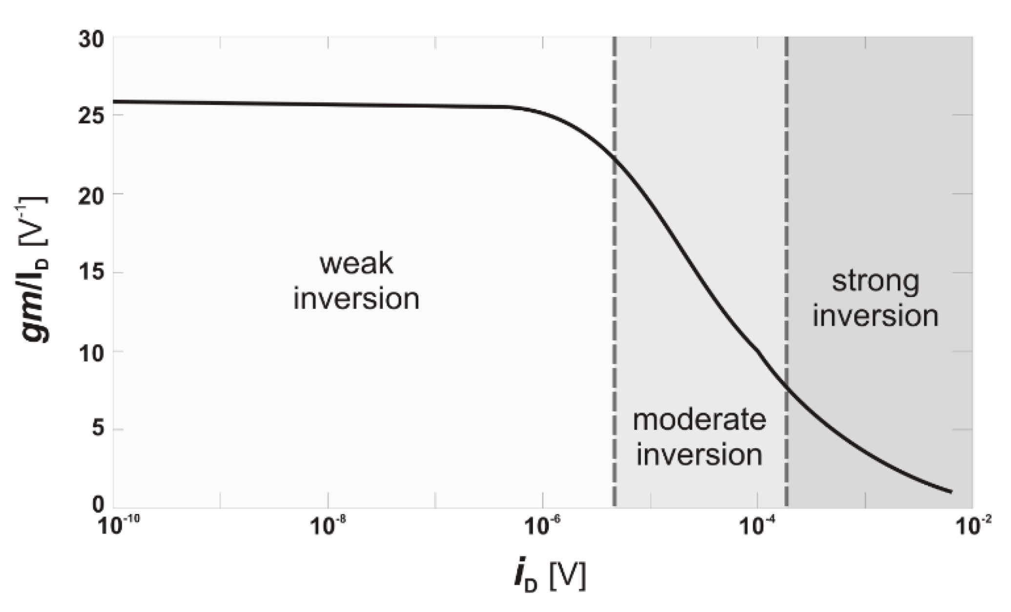
Fig: Transconductance that can be obtained for the input transistor as an EKV function of the Inversion Coefficient (IC). The asymptotes for the velocity without and with velocity saturation are shown.

Acknowledgments: The authors would like to acknowledge the Medipix Collaborations for their continuous support in the design of hybrid pixel detector readout chips.

Aug 10, 2021

[paper] Systematic approach for IG-FinFET amplifier design using gm/Id method

Alireza Hassanzadeh and Sajad Hadidi
Systematic approach for IG-FinFET amplifier design using gm/Id method
Analog Integrated Circuits and Signal Processing (2021)
https://doi.org/10.1007/s10470-021-01917-9

EE Department, Shahid Beheshti University, Tehran, Iran

Abstract: In this paper, a systematic approach has been used to apply gm/Id method for the design of Independent Gate (IG) FinFET amplifiers. The design of high-performance amplifiers using gm/Id method has been successfully applied to nanometer devices. IG-FinFETs have been widely used in digital circuit implementations. However, the application of IG-FinFETs in analog circuits is limited and brings many advantages including low power, low voltage operation of transistors. Independent gates of FinFET can receive different voltages that facilitate low voltage operation of the circuit. Simulation-based gm/Id method has been applied to IG-FinFET transistors and a systematic methodology has been developed for the design of IG-FinFET amplifiers. The Berkeley BSIM-IMG 55 nm technology parameters have been used for HSPICE simulations. The designed amplifier has a DC gain of about 45 dB while consuming 6.5 µW from a single 1 V power supply.

Figgm/Id vs. normalized Id(Vbg)


Apr 13, 2021

[papers] Compact Modeling

[1] Zhang, Yuanke, Tengteng Lu, Wenjie Wang, Yujing Zhang, Jun Xu, Chao Luo, and Guoping Guo. "Characterization and Modeling of Native MOSFETs Down to 4.2 K." arXiv:2104.03094 (2021).

Abstract: The extremely low threshold voltage (VTH) of native MOSFETs (VTH≈0 V @ 300 K) is conducive to the design of cryogenic circuits. Previous research on cryogenic MOSFETs mainly focused on the standard threshold voltage (SVT) and low threshold voltage (LVT) MOSFETs. In this paper, we characterize native MOSFETs within the temperature range from 300 K to 4.2 K. The cryogenic VTH increases up to ∼0.25 V (W/L = 10 µm/10 µm) and the improved subthreshold swing (SS) ≈ 14.30 mV/dec @ 4.2 K. The off-state current (IOFF) and the gate-induced drain leakage (GIDL) effect are ameliorated greatly. The step-up effect caused by the substrate charge and the transconductance peak effect caused by the energy quantization in different subbands are also discussed. Based on the EKV model, we modified the mobility calculation equations and proposed a compact model of large size native MOSFETs suitable for the range of 300 K to 4.2 K. The mobility-related parameters are extracted via a machine learning approach and the temperature dependences of the scattering mechanisms are analyzed. This work is beneficial to both the research on cryogenic MOSFETs modeling and the design of cryogenic CMOS circuits for quantum chips.
Fig: I-V curves of native MOSFETs with W/L= 10/10µm measured (symbol) and calculated (solid line) at various temperatures. (a) Acomparison of the calculation results between this model and the  EKV2.6 model at 77K and 4.2K. (b) Measurement and calculation results of  the output characteristic at 4.2 K.

[2] Qixu Xie  Guoyong Shi; An analytical gm/ID‐based harmonic distortion prediction method for multistage operational amplifiers; Int J Circ Theor Appl. 2021; 1– 27. DOI: 10.1002/cta.3012

Abstract: An analytical stage‐based harmonic distortion (HD) analysis method for multistage operational amplifiers (Op Amps) is developed in this work. This work contributes two fundamental methods that make the analytical HD prediction possible at the circuit level. Firstly, we propose that the traditionally used first order small‐signal transistor quantities gm (transconductance) and go (output conductance) in the gm/ID design methodology for bulk complementary metal‐oxide‐semiconductor (CMOS) technology can be extended to the higher order quantities gm(k) and go(k) (k=1,2,3). With proper normalization, these quantities become neutral to the device dimensions and operation currents, hence can be precharacterized by sweeping simulations and used as lookup tables. Secondly, we further develop analytical nonlinearity expressions for a set of commonly used amplifier stages, represented as the functions of the nonlinearity parameters gm(k) and go(k) of the transistors that form a stage circuit. A combination of these two fundamental methods on hierarchical nonlinearity modeling enables us to apply the existing analytical HD estimation methods for the stage‐form macromodels to predict the circuit‐level HD behavior, overcoming the need of running repeated simulations under device resizing and rebiasing. The proposed harmonic distortion analysis method has been validated by application to real multistage amplifiers, achieving HD prediction results in excellent agreement to fully transistor‐level circuit simulation results but with substantial speedup.

Nov 24, 2020

[paper] Compact Models for Sizing Based on ANN

Husni Habal, Dobroslav Tsonev, Matthias Schweikardt 
Compact Models for Initial MOSFET Sizing Based on Higher-order Artificial Neural Networks
ACM/IEEE Workshop on Machine Learning for CAD (MLCAD ’20)
Nov. 16–20, 2020, Virtual Event, Iceland. ACM, pp. 111-116
DOI: 10.1145/3380446.3430632
1Infineon Technologies AG Munich, Germany
2LogiqWorks Ltd. Sofia, Bulgaria
3Reutlingen University Reutlingen, Germany


Abstract: Simple MOSFET models intended for hand analysis are inaccurate in deep sub-micrometer process technologies and in the moderate inversion region of device operation. Accurate models, such as BSIM6 model, are too complex for use in hand analysis and are intended for circuit simulators. Artificial neural networks (ANNs) are efficient at capturing both linear and non-linear multivariate relationships. In this work, a straightforward modeling technique is presented using ANNs to replace the BSIM model equations. Existing open-source libraries are used to quickly build models with error rates generally below 3%. When combined with a novel approach, such as the gm/Id systematic design method, the presented models are sufficiently accurate for use in the initial sizing of analog circuit components without simulation.

FIG
Figure: ANN Model Architecture.

Oct 6, 2020

[paper] gm/ID-Based Sizing for Analog ICs

Tuotian Liao and Lihong Zhang
An LDE-Aware gm/ID-Based Hybrid Sizing Method for Analog Integrated Circuits
Analog Integrated Circuits. IEEE Transactions on Computer-Aided Design of Integrated Circuits and Systems, 1–1. doi:10.1109/tcad.2020.3025068 

Abstract: Layout-dependent effects (LDEs) have become increasingly more important in the synthesis of analog integrated circuits. In this paper, a two-phase hybrid sizing method for high performance analog circuits is proposed. It consists of gm/ID-based device characterization, circuit modeling, sensitivity-based constraints for LDEs, and mixed-integer nonlinear programming in the first phase, and many-objective evolutionary algorithm (many OEA) based sizing in the second phase. In the first phase, accurate device characterization is handled with little modeling effort thanks to the gm/ID design methodology. Then the LDE parameters that are linked to the normalized DC current are further optimized with the aid of sensitivity analysis. Thus, a variety of electrical, geometrical, and LDE-related constraints can be conveniently integrated into modeling of the sizing problem. In the second phase, the many OEA-based sizing refiner can further optimize the LDE parameters by using more detailed layout information via our proposed model. A new floor plan variation scheme is also applied to improve computation efficiency and enhance optimization effectiveness. The experimental results demonstrate high efficacy of our proposed methodology in LDE-aware analog sizing optimization.
Fig: Module-level of the LDE-aware gm/ID EA two-phase synthesis flow

Thanks to the contribution of the EKV model [1], inversion coefficient (IC) can be used to indicate the biasing inversion level of a MOSFET. This helped Binkley et al. [2] change the design freedom from the conventional W, L, and ID to IC, L, and ID. Since IC is related to DC bias, device geometry, and device characteristics (e.g., gm/ID), it can reflect performance tradeoff (e.g., intrinsic gain vs. bandwidth) of a single MOSFET. In [3], bias information rather than gm/ID parameters was set as variables, while a small-scale LUT was built to find MOSFET aspect ratio (i.e., W/L) and eventually W.

Aknowlegement: This work was supported in part by the Natural Sciences and Engineering Research Council of Canada (NSERC), Canada Foundation for Innovation (CFI), Research and Development Corporation (RDC) of Newfoundland and Labrador, and Memorial University of Newfoundland.

References:
  1. C. Enz, F. Chicco, and A. Pezzotta, “Nanoscale MOSFET modeling: Part 1: The simplified EKV model for the design of low-power analog circuits,” IEEE Solid-State Circuits Mag., vol. 9, no. 3, pp. 26–35, 2017.
  2. D. M. Binkley, C. E. Hopper, S.D. Tucker, B.C. Moss, J. M. Rochelle, and, D. P. Foty, “A CAD methodology for optimizing transistor current and sizing in analog CMOS design,” IEEE Trans. Comput-Aided Design Integr. Circuits Syst., vol. 22 no. 2, pp. 225-237, 2003.
  3. C.-W. Lin, P.-D. Sue, Y.-T. Shyu, and S.-J. Chang, “A bias-driven approach for automated design of operational amplifiers,” in Proc. Int.

May 18, 2020

[paper] Novel Design and Optimization and the gm/ID Ratio

A Novel Design and Optimization Approach for Low Noise Amplifiers (LNA) Based on MOST Scattering Parameters and the gm/ID Ratio
1Facultad de Ingeniería, Universidad Católica de Córdoba, Córdoba 5017 (AN)
2Service d’Électronique et Microélectronique, Université de Mons (UMONS), 7000 Mons (BE)
3Departamento de Electrónica, Instituto de Astrofísica de Canarias (IAC), 38200 La Laguna (SP)
* Author to whom correspondence should be addressed.
Electronics 2020, 9(5), 785; https://doi.org/10.3390/electronics9050785
Received: 31 March 2020 / Revised: 30 April 2020 
Accepted: 9 May 2020 / Published: 11 May 2020

AbstractThis work presents a new design methodology for radio frequency (RF) integrated circuits based on a unified analysis of the scattering parameters of the circuit and the gm/ID ratio of the involved transistors. Since the scattering parameters of the circuits are parameterized by means of the physical characteristics of transistors, designers can optimize transistor size and biasing to comply with the circuit specifications given in terms of S-parameters. A complete design of a cascode low noise amplifier (LNA) in 65nm CMOS technology is taken as a case study in order to validate the approach. In addition, this methodology permits the identification of the best trade-off between the minimum noise figure and the maximum gain for the LNA in a very simple way.
Figure: gm/ID versus iD

Acknowledgement - This research was funded by Universidad Católica de Córdoba (Argentina), the Walloon Region DGO6 BEWARE Fellowships Academia Programme (1410164-POHAR, cofunded by the European Marie Curie Actions), the Belgian FNRS (Fond National pour la Recherche Scientifique) and the Argentinean MINCyT (Ministerio de Ciencia y Tecnología).

Jan 10, 2019

An Empirical Model to Enhance the Flexibility of gm/Id Tuning in BSIM-BULK Model

Ravi Goel, Chetan Gupta, Yogesh S. Chauhan
EE Department, Indian Institute of Technology Kanpur, Kanpur, India
Published in: 2018 5th IEEE Uttar Pradesh Section International Conference on Electrical, Electronics and Computer Engineering (UPCON)

Abstract: Recent enhancement in BSIM-BULK (formerly BSIM6) model is presented in this work. The industry standard models like BSIM4, PSP, BSIM-BULK etc. lack the parameters for tuning of transconductance to channel current ratio (gm/Id). gm/Id is also a critical figure of merit for analog applications. Here, we propose an empirical model to enhance the flexibility of gm/Id tuning behavior. The proposed model provides good fitting for different channel lengths and drain bias.

Paper Sections:
I. Introduction
II. An Empirical Model for gm/Id Tuning
III. Model Implementation
IV. Model Validation with TCAD
V. Conclusion

Source:
DOI: 10.1109/UPCON.2018.8597065

Sep 12, 2017

[book] Systematic Design of Analog CMOS Circuits

Paul G. A. Jespers, Boris Murmann
Cambridge University Press; 31 Oct 2017; 342pp

Discover a fresh approach to efficient and insight-driven analog integrated circuit design in nanoscale-CMOS with this hands-on guide. Expert authors present a sizing methodology that employs SPICE-generated lookup tables, enabling close agreement between hand analysis and simulation. This enables the exploration of analog circuit tradeoffs using the gm/ID ratio as a central variable in script-based design flows, and eliminates time-consuming iterations in a circuit simulator. Supported by downloadable MATLAB code, and including over forty detailed worked examples, this book will provide professional analog circuit designers, researchers, and graduate students with the theoretical know-how and practical tools needed to acquire a systematic and re-use oriented design style for analog integrated circuits in modern CMOS.

Nov 15, 2016

[paper] Analysis of aging effects - From transistor to system level

Analysis of aging effects - From transistor to system level
Maike Taddiken*, Nico Hellwege, Nils Heidmann, Dagmar Peters-Drolshagen, Steffen Paul
Institute of Electrodynamics and Microelectronics,
University of Bremen, Otto-Hahn-Allee 1, Bremen 28359,Germany

ABSTRACT: Due to shrinking feature sizes in integrated circuits, additional reliability effects have to be considered which influence the functionality of the system. These effects can either result from the manufacturing process or external influences during the lifetime such as radiation and temperature. Additionally, modern technology nodes are affected by time-dependent degradation i.e. aging. Due to the age-dependent degradation of a circuit, processes on the atomic scale of the semiconductor material lead to charges in the oxide silicon interface of CMOS devices, altering the performance parameters of the device and subsequently the behavior of the circuit. With the continuous downscaling of modern semiconductor technologies, the impact of these atomic scale processes affecting the overall system characteristics becomes more and more critical. Therefore, aging effects need to be assessed during the design phase and actions have to be taken guaranteeing the correct system functionality throughout a system’s lifetime. This work presents methods to investigate the influence of age-dependent degradation as well as process variability on different levels. An operating-point dependent sizing methodology based on the gm/ID method extended to incorporate aging, which aims at developing aging-resistent circuits is presented. The basic idea of the gm/ID sizing method is the dependence of the operating point of a MOS transistor on the state of inversion in the channel, its strong relation to circuit performance and the possibility to calculate transistor dimensions.The inversion coefficient IC is a fundamental metric within the gm/ID method and numerically represents the inversion level of a MOS device formally described in the EKV MOS model. Additionally, the sensitivity of circuit performances in regard to aging can be determined. In order to investigate the reliability of a complex system on behavioral level, a modeling method to represent the performance of system components in dependence of aging and process variability is introduced. [read more...]

Nov 11, 2015

[ESSCIRC 2015] Low-power analog RF circuit design based on the inversion coefficient

[ref] Enz, Christian; Chalkiadaki, Maria-Anna; Mangla, Anurag, "Low-power analog/RF circuit design based on the inversion coefficient," in ESSCIRC 2015 - 41st , vol., no., pp.202-208, 14-18 Sept. 2015

Abstract: This paper discusses the concept of the inversion coefficient as an essential design parameter that spans the entire range of operating points from weak via moderate to strong inversion, including velocity saturation. Several figures-of-merit based on the inversion coefficient, especially suitable for the design of low-power analog and RF circuits, are presented. These figures-of-merit incorporate the various trade-offs encountered in analog and RF circuit design. The use of the inversion coefficient and the derived figures-of-merit for optimization and design is demonstrated through simple examples. Finally, the simplicity of the inversion coefficient based analytical models is emphasized by their favorable comparison against measurements of a commercial 40-nm bulk CMOS process as well as with simulations using the BSIM6 model.

Keywords: Analytical models, Integrated circuits, Noise, Radio frequency, Silicon, Transconductance, Transistors, BSIM6

URL / doi: 10.1109/ESSCIRC.2015.7313863