Showing posts with label VLSI. Show all posts

Feb 28, 2024

[FOSSDEM 2024] Open PDK Initiative

FOSDEM 2024 was a two-day event organized by volunteers to promote the widespread use of free and open source software. Took place at the ULB Solbosch campus in the beautiful city of Brussels (Belgium), FOSDEM is widely recognized as the best FOSS conference in Europe.

There were two DevRooms to discuss the status and further FOSS CAD/EDA IC design tools developments and open PDK initiative:

FOSDEM'24 Inauguration Session

Jan 3, 2024

VLSID 2024 Conference


PULP Platform @pulp_platform (5h)
Cheers to 2024! The 37th International Conference on VLSI Design will start in Kolkata on Monday. @LucaBenini will give a banquet talk titled "Open Platform for the Embodied AI Era" at 7:10 PM (IST) on January 9. Check out the conference website for tutorials and schedule: https://vlsid.org

In the present era of automation and connected things, VLSI technology armed with AI and Quantum could be pivotal in changing the VLSI landscape starting from manufacturing to devices to design. To elaborate on this paradigm shift, the theme 2024 VLSI Design conference is aptly chosen to be “VLSI meets AI and Quantum for Cyber Physical Systems”.

Over a span of five-days of VLSID2024, the summit will feed brains and nurture minds with state-of-the-art exhibitors, presentations, panel discussions, innovation forums, and tutorials by established technologists.

May 30, 2023

[PhD Thesis] Digital-based analog processing in nanoscale CMOS ICs for IoT applications

Digital-based analog processing in nanoscale CMOS ICs for IoT applications
http://hdl.handle.net/10183/249786
PhD Cadndiate: Pedro Filipe Leite Correia De Toledo
Universidade Federal do Rio Grande do Sul. Instituto de Informática
Programa de Pós-Graduação em Microeletrônica.
Advisor: Klimach, Hamilton Duarte
Co-advisor: Crovetti, Paolo Stefano

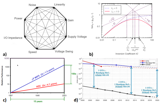
Abstract: The Internet-of-Things (IoT) concept has been opening up a variety of applications, such as urban and environmental monitoring, smart health, surveillance, and home automation. Most of these IoT applications require more and more power/area efficient Complemen ary Metal–Oxide–Semiconductor (CMOS) systems and faster prototypes (lower time-to market), demanding special modifications in the current IoT design system bottleneck: the analog/RF interfaces. Specially after the 2000s, it is evident that there have been significant improvements in CMOS digital circuits when compared to analog building blocks. Digital circuits have been taking advantage of CMOS technology scaling in terms of speed, power consumption, and cost, while the techniques running behind the analog signal processing are still lagging. To decrease this historical gap, there has been an increasing trend in finding alternative IC design strategies to implement typical analog functions exploiting Digital in-Concept Design Methodologies (DCDM). This idea of re-thinking analog functions in digital terms has shown that Analog ICs blocks can also avail of the feature-size shrinking and energy efficiency of new technologies. This thesis deals with the development of DCDM, demonstrating its compatibility for Ultra-Low-Voltage (ULV) and Power (ULP) IoT applications. This work proves this statement through the proposing of new digital-based analog blocks, such as an Operational Transconductance Amplifiers (OTAs) and an ac-coupled Bio-signal Amplifier (BioAmp). As an initial contribution, for the first time, a silicon demonstration of an embryonic Digital-Based OTA (DB-OTA) published in 2013 is exhibited. The fabricated DB-OTA test chip occupies a compact area of 1,426 µm2 , operating at supply voltages (VDD) down to 300 mV, consuming only 590 pW while driving a capacitive load of 80pF. With a Total Harmonic Distortion (THD) lower than 5% for a 100mV input signal swing, its measured small-signal figure of merit (FOMS) and large-signal figure of merit (FOML) are 2,101 V −1 and 1,070, respectively. To the best of this thesis author’s knowledge, this measured power is the lowest reported to date in OTA literature, and its figures of merit are the best in sub-500mV OTAs reported to date. As the second step, mainly due to the robustness limitation of previous DB-OTA, a novel calibration-free digital-based topology is proposed, named here as Digital OTA (DIG OTA). A 180-nm DIGOTA test chip is also developed exhibiting an area below the 1000 µm2 wall, 2.4nW power under 150pF load, and a minimum VDD of 0.25 V. The proposed DIGOTA is more digital-like compared with DB-OTA since no pseudo-resistor is needed. As the last contribution, the previously proposed DIGOTA is then used as a building block to demonstrate the operation principle of power-efficient ULV and ultra-low area (ULA) fully-differential, digital-based Operational Transconductance Amplifier (OTA), suitable for microscale biosensing applications (BioDIGOTA) such as extreme low area Body Dust. Measured results in 180nm CMOS confirm that the proposed BioDIGOTA can work with a supply voltage down to 400 mV, consuming only 95 nW. The BioDIGOTA layout occupies only 0.022 mm2 of total silicon area, lowering the area by 3.22X times compared to the current state of the art while keeping reasonable system performance, such as 7.6 Noise Efficiency Factor (NEF) with 1.25 µVRMS input-referred noise over a 10 Hz bandwidth, 1.8% of THD, 62 dB of the common-mode rejection ratio (CMRR) and 55 dB of power supply rejection ratio (PSRR). After reviewing the current DCDM trend and all proposed silicon demonstrations, the thesis concludes that, despite the current analog design strategies involved during the analog block development

Fig: a) analog design octagon; b) gm/ID·fT versus the inversion coefficient IC, λc is the parameter corresponding to the fraction of the channel in which the carrier drift velocity reaches the saturated velocity over a portion of the channel geometrical length; c) Performance difference between analog and digital blocks over time; d) Area reduction over the years of the bitcell SRAM, OTA and bandgap reference

May 8, 2021

10th All-Russia MES-2021 Conference

10th All-Russia Science and Technology Conference
Problems of Advanced Micro- and Nanoelectronic Systems Development 
MES-2021
March - November 2021
Moscow | Zelenograd

MES-2021 is dedicated to urgent issues of design automation of microelectronic systems, SoC, IP-blocks and a new element base of micro-and nanoelectronics. These issues have been and remain actual to science and technology, as evidenced by the major topics of the Annual International Conference on CAD and the development of micro-and nanoelectronic devices. MES is the largest conference in the field of CAD microelectronics in Russia and CIS countries. Proceedings of the MES conference is included in HAC list (issue 23.03.2021, pos. 2017) of Russian scientific journals, where should be published the main results of the PhD and DSc theses.
The upcoming 10th MES-2021 conference will be held mainly in the correspondence format, starting on March 01, 2021, and it will be concluded with its plenary session in November 2021.

Key discussion topics
1. Theoretical aspects of micro-and nanoelectronic systems (MES).
2. Methods and tools of design automation for micro-and nanoelectronic circuits and systems (VLSI CAD).
3. Experience of development of digital, analog, digital to analog, radio functional blocks of VLSI.
4. Features of VLSI design for nanometer technologies.
5. SoCs for advanced radioelectronic equipment.
6. Exhibition and presentation of commercial products.

Fields of interest of the conference include (but is not limited to) the following topics of relevant studies of VLSI design and VLSI design automation techniques:

Design
1. Circuits and Systems based on nanometer technologies
2. Systems on Chip
3. Digital VLSI Design
4. Design of analog functional blocks and radio VLSI
5. Design of mixed-signal VLSI
6. Methods of structural synthesis of analog, digital and mixed VLSI and complex functional blocks
7. Specialized (resistant to special effects, photosensitivity, etc.) VLSI

Simulation
1. Methods of simulation of digital, analog and mixed circuits and systems
2. Methods for radio VLSI simulation
3. Structural, logical, circuit, mixed and layout simulation
4. Methods for generating models and macromodels for VLSI CAD
5. Device and Technology simulation
6. Behavioral simulation

Information processing methods
1. Information coding
2. Digital data processing
3. Use of artificial intelligence methods, neural networks, etc. in micro- and nanoelectronic system designs
4. Unconventional arithmetic
5. High-performance computers

The development of nanoelectronic systems on new principles
1. Nanomagnetic storage devices
2. Magnetosensor structures

Call for participation in the conference program
I stage - After registration at least one of the co-authors of the report one can send an article. To do this, using their registration data, please log in (see upper right corner of screen). Fill in all required fields. On the website you should send a file containing the main text of the article (in Russian or English) and an extended abstract in English (if the main text is in Russian) or a simple abstract in Russian (if the main text of the article in English). Requirements for the articles sent to MES.
II stage - sending additional documents only for the articles, which have been reviewed and accepted to the conference program.

Visit the 10th MES-2021 conference website at: http://www.mes-conference.ru/index.php


May 3, 2021

[paper] FET Library for VLSI

Taehak Kim1, Jaehoon Jeong2, Seungmin Woo2, Jeonggyu Yang1, Hyunwoo Kim2 Ahyeon Nam2, Changdong Lee2, Jinmin Seo2, Minji Kim2, Siwon Ryu2, Yoonju Oh2, and Taigon Song1,2  
NS3K : A 3nm Nanosheet FET Library for VLSI Prediction in Advanced Nodes 
IEEE ISCAS, 2021, pp. 1-5, DOI 10.1109/ISCAS51556.2021.9401055.

1School of Electronics Engineering, Kyungpook National University (KNU), Daegu 41566, South Korea
2School of Electronic and Electrical Engineering, Kyungpook National University (KNU), Daegu 41566, South Korea


Abstract: Nanosheet FETs (NSFETs) are expected as future devices that replace FinFETs beyond the 5nm node. Despite the importance of the devices, few studies report the impact of NSFETs in the full-chip level. Therefore, this paper presents NS3K, the first 3nm NSFET library, and presents the results in a full-chip scale. Based on our results, 3nm NSFET reduces power by -27.4%, total wirelength by -25.8%, number of cells by -8.5%, and area by -47.6% over 5nm FinFET, respectively, due to better devices and interconnect scaling. However, careful device/layout designs followed by routing-resource considering standard cells are required to maximize the advantages of 3nm technology. 

Fig: Projected 3nm NSFET library development flow. Upper side of each step shows the names of required tools. Each colored-boxes correspond to the steps required for specific tasks: The blue boxes - device development, the orange boxes - digital design, and the green boxes - back end design, respectively.

Acknowledgements: This research was supported by National R&D Program through the National Research Foundation of Korea (NRF) funded by Ministry of Science and ICT (2020M3H2A1078045). The EDA tool was supported by the IC Design Education Center(IDEC), Korea. This work was supported by the National Research Foundation of Korea (NRF) grant funded by the Korea government (MSIT) (No.2019R1G1A109470212).


Apr 29, 2021

[PhD] VLSI Interconnect Reliability

Shaoyi Peng
Modeling and Simulation Methods for VLSI Interconnect Reliability Focusing 
on Time Dependent Dielectric Breakdown
PhD Dissertation in Electrical Engineering
University of California Riverside
https://escholarship.org/uc/item/966241xk (March 2021)

Abstract: Time dependent dielectric breakdown (TDDB) is one of the important failure mechanisms for Copper (Cu) interconnects that are used in VLSI circuits. This reliability effect becomes more severe as the space between wires is shrinking and low-k dielectric materials (low electrical and mechanical strength) are used. There are many studies and theories focusing on the physics of it. However, there is limited research from the electronics design automation (EDA) perspective on this topic, aiming to evaluate, or alleviate it from the perspective of designing a VLSI chip. This thesis compiles several studies into evaluating TDDB on the circuit level, and engineering methods that help the evaluation. The first work extends the study of a published physics model on simplified yet practical cases. It simplifies the calculation of lifetime by deriving an analytic solution and applying fitting methods. The second study proposes a new way to evaluate lifetime of a chip by extending the models of simple interconnect structures to the complete chip. This method is more robust as it focuses more on a complete chip. However, heavy dependence of finite element method (FEM) makes the flow very slow. The third study adopts machine learning methods to accelerate this slow evaluation process. The proposed method is also applicable to other similar electrostatics applications. Last but not least, the fourth study focuses on a GPU based LU factorization algorithm, which, on a broader aspect, is a universal numerical algorithm used in many different simulation applications, which can be helpful to TDDB evaluations as it can be used in FEM.
Fig: Structure of two copper interconnect wires and the IMD in the cross-section SEM image after TDDB failure [sem]
REF
[sem] N. Suzumura, S. Yamamoto, D. Kodama, K. Makabe, J. Komori, E. Murakami, S. Maegawa, and K Kubota. A new TDDB degradation model based on Cu ion drift in Cu interconnect dielectrics. In IEEE Int. Reliability Physics Symposium (IRPS), pages 26–30, 2006.

Mar 9, 2021

[RIP] prof. dr hab. inż. Andrzej Jakubowski

Professor Andrzej Jakubowski was born in 1940 in Kraków; died on March 9, 2021 in Warsaw. He was a graduate of the TU Warsaw. He obtained his PhD in 1974, and his habilitation (DSc) in 1983. Six years later, he was awarded the academic professor title. During his scientific and research carrier, he was the author or co-author of about 650 scientific papers, conference contributions and books (including [1]), 9 patents and patent applications, as well as promoting popular science. Professor Jakubowski was one of the most outstanding TU Warsaw professors, co-founder of the Polish microelectronics industry. He was also a pioneer of diamond-like and graphene layers application in microelectronics. For more than 50 years associated with the Institute of Microelectronics and Optoelectronics as its Director; founder of an outstanding scientific school of the micro and nanoelectronics, higly recognized in Poland as well as by many foreign R&D centers; a teacher and tutor of next generations of engineers; personally devoted to young people; with deep passion for half a century educating students and scientific staff at the highest international level with immense dedication of all his heart and scientific knowledge. Professor Jakubowski promoted 23 PhD students and may of them are working for international semiconductor companies and R&D organizations, now.

In the years 2004-2008 at the Warsaw University of Technology he was the director of the Institute of Microelectronics and Optoelectronics. Previously, he headed the Department of Microelectronics and the Department of Microelectronics and Nanoelectronics at this Institute. Between 1989 and 1992, he was the director of the Institute of Electron Technology (ITE, Warsaw; now Lukasiewicz IMiF). He was a member of the Electronics and Telecommunications Committee of the Polish Academy of Sciences. In 2014, Professor Jakubowski was awarded the honorary title of doctor honoris causa of TU Lodz. For his achievements in scientific and didactic work, he has received, among many others, the award of the Faculty of Technical Sciences of the Polish Academy of Sciences (PAN) and the Awards of the Minister of Science and Higher Education.

REF:
[1] Andrzej Jakubowski, Wieslaw Marciniak, Henryk M. Przewlocki; Diagnostic Measurements in LSI/VLSI Integrated Circuits Production; World Scientific, 30 Apr 1991; Technology & Engineering; 372pp

Jul 12, 2019

IEEE ICECS 2019 paper submission deadline

ICECS 2019 paper deadline submission is approaching fast: July 15th, 2019

Please distribute this reminder to possible contributors and interested researchers and colleagues. Topics of interest include but are not limited to:

• Analog/mixed-signal/RF circuits
• Biomedical and Bio-Inspired Circuits and Systems
• EDA, Test and Reliability
• Digital circuits and systems
• Linear and Non-linear Circuits
• Low-Power Low-Voltage Design
• Microsystems
• Neural networks, Machine and Deep Learning
• Sensors and Sensing Systems
• Signal Processing, Image and Video
• VLSI Systems and Applications

The technical committee invites authors to submit 4-page papers in standard IEEE double-column format, including references, figures and tables, to clearly present the work, methods, originality, significance and applications of the techniques discussed.

Maurizio Valle; IEEE ICECS 2019 General Chair
https://www.ieee-icecs2019.org/

Feb 28, 2017

[paper] Readout electronics for LGAD sensors

Readout electronics for LGAD sensors
O. Alonso,a N. Franch,a J. Canals,a F. Palacio,a M. López,a A. Vilà,a A. Diéguez,a
M. Carulla,b D. Flores,b S. Hidalgo,b A. Merlos,b G. Pellegrinib and D. Quirionb
aDepartment of Engineering: Section of Electronics, University of Barcelona,
C/ Martí i Franquès nº1, Barcelona, 08028 Spain
bInstituto de Microelectrónica de Barcelona — Centro Nacional de Microelectrónica (IMB-CNM),
Campus UAB, Cerdanyola del Vallès, Bellaterra, Barcelona, 08193 Spain
doi:10.1088/1748-0221/12/02/C02069

Abstract: In this paper, an ASIC fabricated in 180 nm CMOS technology from AMS with the very front-end electronics used to readout LGAD sensors is presented as well as its experimental results. The front-end has the typical architecture for Si-strip readout, i.e., preamplification stage with a Charge Sensitive Amplifier (CSA) followed by a CR-RC shaper. Both amplifiers are based on a folded cascode structure with a PMOS input transistor and the shaper only uses passive elements for the feedback stage. The CSA has programmable gain and a configurable input stage in order to adapt to the different input capacitance of the LGAD sensors (pixelated, short and long strips) and to the different input signal (depending on the gain of the LGAD). The fabricated prototype has an area of 0.865mm  0.965mm and includes the biasing circuit for the CSA and the shaper, 4 analog channels (CSA+shaper) and programmable charge injection circuits included for testing purposes. A first approach to find the proper dimensioning of the input transistor has been done using a Matlab script, where the transconductance value has been calculated with the EKV model

Acknowledgments This work has been partially funded by the Spanish national projects FPA2013-48387 and FPA2015-71292. In addition, this work has been done in the framework of RD50 CERN collaboration.

Jun 15, 2016

[book] Compact Models for Integrated Circuit Design

 Compact Models for Integrated Circuit Design: 
 Conventional Transistors and Beyond
 Samar K. Saha
Taylor & Francis, 26 Aug 2015 - Technology & Engineering - 545 pages - ISBN 9781482240665

Compact Models for Integrated Circuit Design: Conventional Transistors and Beyond provides a modern treatise on compact models for circuit computer-aided design (CAD). Written by an author with more than 25 years of industry experience in semiconductor processes, devices, and circuit CAD, and more than 10 years of academic experience in teaching compact modeling courses, this first-of-its-kind book on compact SPICE models for very-large-scale-integrated (VLSI) chip design offers a balanced presentation of compact modeling crucial for addressing current modeling challenges and understanding new models for emerging devices.
Starting from basic semiconductor physics and covering state-of-the-art device regimes from conventional micron to nanometer, this text:
  • Presents industry standard models for bipolar-junction transistors (BJTs), metal-oxide-semiconductor (MOS) field-effect-transistors (FETs), FinFETs, and tunnel field-effect transistors (TFETs), along with statistical MOS models
  • Discusses the major issue of process variability, which severely impacts device and circuit performance in advanced technologies and requires statistical compact models
  • Promotes further research of the evolution and development of compact models for VLSI circuit design and analysis
  • Supplies fundamental and practical knowledge necessary for efficient integrated circuit (IC) design using nanoscale devices
  • Includes exercise problems at the end of each chapter and extensive references at the end of the book

Compact Models for Integrated Circuit Design: Conventional Transistors and Beyond is intended for senior undergraduate and graduate courses in electrical and electronics engineering as well as for researchers and practitioners working in the area of electron devices. However, even those unfamiliar with semiconductor physics gain a solid grasp of compact modeling concepts from this book. [more...]

Feb 22, 2016

Alliance: FOSS VLSI/CAD System


Alliance is a complete set of free cad tools and portable libraries for VLSI design. It includes a VHDL compiler and simulator, logic synthesis tools, and automatic place and route tools. A complete set of portable CMOS libraries is provided. Alliance is the result of a twelve year effort spent at SoC department of LIP6 laboratory of the Pierre & Marie Curie University (Paris VI, France). Alliance has been used for research projects such as the 875 000 transistors StaCS superscalar microprocessor and 400 000 transistors IEEE Gigabit HSL Router.

Alliance VLSI CAD System is free software. Binaries, source code and cells libraries are freely available under the GNU General Public License (GPL). You are welcome to use the software package even for commercial designs without any fee. You are kindly requested to mention: "Designed with Alliance © LIP6, Université Pierre et Marie Curie".

ICs Designed with Alliance
  • Smartlabs/Smarthome designed a complete circuit in the XFAB XH035 technology (2014).
  • Tokai University (Shimizu Lab) designed the SNX, a 16 bits processor in the ROHM 0.18µm (2010).
Useful Links

Oct 26, 2014

EDS VLSI Technology and Circuits TC Report

 EDS VLSI Technology and Circuits Technical Committee Report

The VLSI Technology and Circuits Technical Committee was formed in 1998 under the leadership of Professor Charles G. Sodini (MIT) and followed by Dr. H.-S. Philip Wong (IBM), Werner Weber (Infineon), Dr. James A. Hutchby (SRC) and Dr. Bin Zhao (Freescale Semiconductor). Since its formation, the VLSI Committee has made it their mission to identify new technical trends, help foster new technical concepts, and serve the emerging needs of the Electron Devices and Solid-State Circuits communities in VLSI. The committee members include many well recognized technical experts representing a very wide spectrum of technical expertise in VLSI devices, technology, and circuits. Every year the committee brainstorms (by email), ideas that are suitable for new workshops, special issues for a journals, panel sessions, and special sessions for conferences. Committee members then drive these ideas forward and find a way to make them happen; either by being the organizers themselves, or by finding suitable organizers for the topic. They work closely together with journal editors and conference organizers. It is much easier to attach new workshops to existing conferences, than to establish new conferences. 

[read more at http://eds.ieee.org/eds-newsletters.html]