Showing posts with label Transient analysis. Show all posts

May 1, 2020

[paper] Physical Mechanisms of Reverse DIBL and NDR in FeFETs With Steep Subthreshold Swing

C. Jin, T. Saraya, T. Hiramoto and M. Kobayashi,
in IEEE J-EDS, vol. 8, pp. 429-434, 2020
doi: 10.1109/JEDS.2020.2986345

Abstract - We have investigated transient IdVg and IdVd characteristics of ferroelectric field-effect transistor (FeFET) by simulation with ferroelectric model considering polarization switching dynamics. We show transient negative capacitance (TNC) with polarization reversal and depolarization effect can result in sub-60mV/dec subthreshold swing (SS), reverse drain-induced barrier lowering (R-DIBL), and negative differential resistance (NDR) without traversing the quasi-static negative capacitance (QSNC) region of the S-shaped polarization-voltage (PV) predicted by single-domain Landau theory. Moreover, the mechanisms of R-DIBL and NDR based on the TNC theory are discussed in detail. The results demonstrated in this work can be a possible explanation for the mechanism of previously reported negative capacitance field-effect transistor (NCFET) with sub-60mV/dec SS, R-DIBL, and NDR.
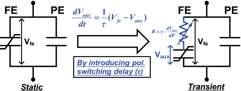
Equivalent circuits of a ferroelectric capacitor in both static and transient conditions.

Oct 17, 2017

[paper] Accurate diode behavioral model with reverse recovery

Stanislav Banáša,b, Jan Divínab, Josef Dobešb, Václav Paňkoa
aON Semiconductor, SCG Czech Design Center, Department of Design System Technology, 1. maje 2594, 756 61 Roznov pod Radhostem, Czech Republic
bCzech Technical University in Prague, Faculty of Electrical Engineering, Department of Radioelectronics, Technicka 2, 166 27 Prague 6, Czech Republic
Volume 139, January 2018, Pages 31–38

Highlights:

  • The complex robust time and area scalable Verilog-A model of diode containing reverse recovery effect has been developed.
  • Due to implemented reverse recovery effect the model is useful especially for high-speed or high-voltage power devices.
  • The model can be used as stand-alone 2-terminal diode or as a parasitic p-n junction of more complex lumped macro-model.
  • Two methods of model parameter extraction or model validation have been demonstrated.

ABSTRACT: This paper deals with the comprehensive behavioral model of p-n junction diode containing reverse recovery effect, applicable to all standard SPICE simulators supporting Verilog-A language. The model has been successfully used in several production designs, which require its full complexity, robustness and set of tuning parameters comparable with standard compact SPICE diode model. The model is like standard compact model scalable with area and temperature and can be used as a stand-alone diode or as a part of more complex device macro-model, e.g. LDMOS, JFET, bipolar transistor. The paper briefly presents the state of the art followed by the chapter describing the model development and achieved solutions. During precise model verification some of them were found non-robust or poorly converging and replaced by more robust solutions, demonstrated in the paper. The measurement results of different technologies and different devices compared with a simulation using the new behavioral model are presented as the model validation. The comparison of model validation in time and frequency domains demonstrates that the implemented reverse recovery effect with correctly extracted parameters improves the model simulation results not only in switching from ON to OFF state, which is often published, but also its impedance/admittance frequency dependency in GHz range. Finally the model parameter extraction and the comparison with SPICE compact models containing reverse recovery effect is presented [read more...]

FIG: Solving the recursive calculation of reverse recovery charge

Aug 1, 2017

[paper] Circuit-level simulation methodology for Random Telegraph Noise by using Verilog-AMS


T. Komawaki, M. Yabuuchi, R. Kishida, J. Furuta, T. Matsumoto and K. Kobayashi
Circuit-level simulation methodology for Random Telegraph Noise by using Verilog-AMS
2017 IEEE ICICDT, Austin, TX, USA, 2017, pp. 1-4.
doi: 10.1109/ICICDT.2017.7993526

Abstract: As device sizes are downscaled to nanometer, Random Telegraph Noise (RTN) becomes dominant. It is indespensable to accurately estimate the effect of RTN. We propose the RTN simulation method for analog circuits. It is based on the charge trapping model. We replicate the RTN-induced threshold voltage fluctuation to attach a variable DC voltage source to the gate of MOSFET by using Verilog-AMS. We confirm that drain current of MOSFETs temporally fluctuates. The fluctuations of RTN are different for each MOSFET. Our proposed method can be applied to estimate the temporal impact of RTN including multiple transistors. We can successfully replicate RTN-induced frequency fluctuations in 3-stage ring oscillators as similar as the measurement results [read more...]