Showing posts with label TCAD. Show all posts

Jan 29, 2024

List of the publications using or referring to DEVSIM

List of the publications using or referring to DEVSIM
[1] K. Wang et al.; Design and simulation of a novel 4H-SiC LGAD timing device; Radiation detection technology and methods; (2023) https://doi.org/10.1007/s41605-023-00431-y
[2] J. Lauwaert; Technology computer aided design based deep level transient spectra: Simulation of high-purity germanium crystals; Journal of Physics D: Applied Physics; (2022) https://doi.org/10.1088/1361-6463/ac34ad
[3] Q. Chen et al.; Analytical model for donor like Gaussian traps in organic thin-film transistor; Organic Electronics; (2021) https://doi.org/10.1016/j.orgel.2022.106464
[4] Q. Chen et al.; The Impact of Contact Position on the Retention Performance in Thin-Film Ferroelectric Transistors; Physica Status Solidi A; (2021) https://doi.org/10.1002/pssa.202100408
[5] L. Hulbert; Designing a Simulator for an Electrically-Pumped Organic Laser Diode; Master’s Thesis; (2019) https://doi.org/10.15368/theses.2019.60
[6] J. E. Sanchez and Q. Chen; Element Edge Based Discretization for TCAD Device Simulation; IEEE Transactions on Electron Devices; (2021) https://doi.org/10.1109/TED.2021.3094776
[7] J. Lauwaert; Fill Factor Loss in a Recombination Junction for Monolithic Tandem Solar Cells; ACS Appl. Energy Mater.; (2023) https://doi.org/10.1021/acsaem.3c00041
[8] J. E. Sanchez; DEVSIM: A TCAD Semiconductor Device Simulator; Journal of Open Source Software; (2022) https://doi.org/10.21105/joss.03898
[9] L. Rickert et al.; High-performance designs for fiber-pigtailed quantum-light sources based on quantum dots in electrically-controlled circular Bragg gratings; Optics Express; (2023) https://doi.org/10.1364/OE.486060
[10] L. R. Brennaman & A. J. Samin; Insights into the performance of InAs-based devices in extreme environments from multiscale simulations; Applied Physics A; (2023) https://doi.org/10.1007/s00339-023-06756-1
[11] M. D. K Jones et al.; Modelling Interfaces in Thin-Film Photovoltaic Devices; Frontiers in Chemistry; (2022) https://doi.org/10.3389/fchem.2022.920676
[12] R. Sellers et al.; fabrication and modeling study to reduce valence band offset in HgCdTe MWIR nBn photodetectors grown on silicon using superlattice barriers; Proc. SPIE PC12687, Infrared Sensors, Devices, and Applications XIII,; (2023) https://doi.org/10.1117/12.2677394
[13] TANG Zhenglai and CAO Bingyang ; Simulations of self-heating effects and the heat generation mechanisms in SOI-MOS devices; Microelectronics & Computer; (2023) https://doi.org/10.19304/J.ISSN1000-7180.2023.0630
[14] Kotecha et al.; Modeling Needs for Power Semiconductor Devices and Power Electronics Systems; IEDM (2019) (2019) https://doi.org/10.1109/IEDM19573.2019.8993449

Jan 15, 2024

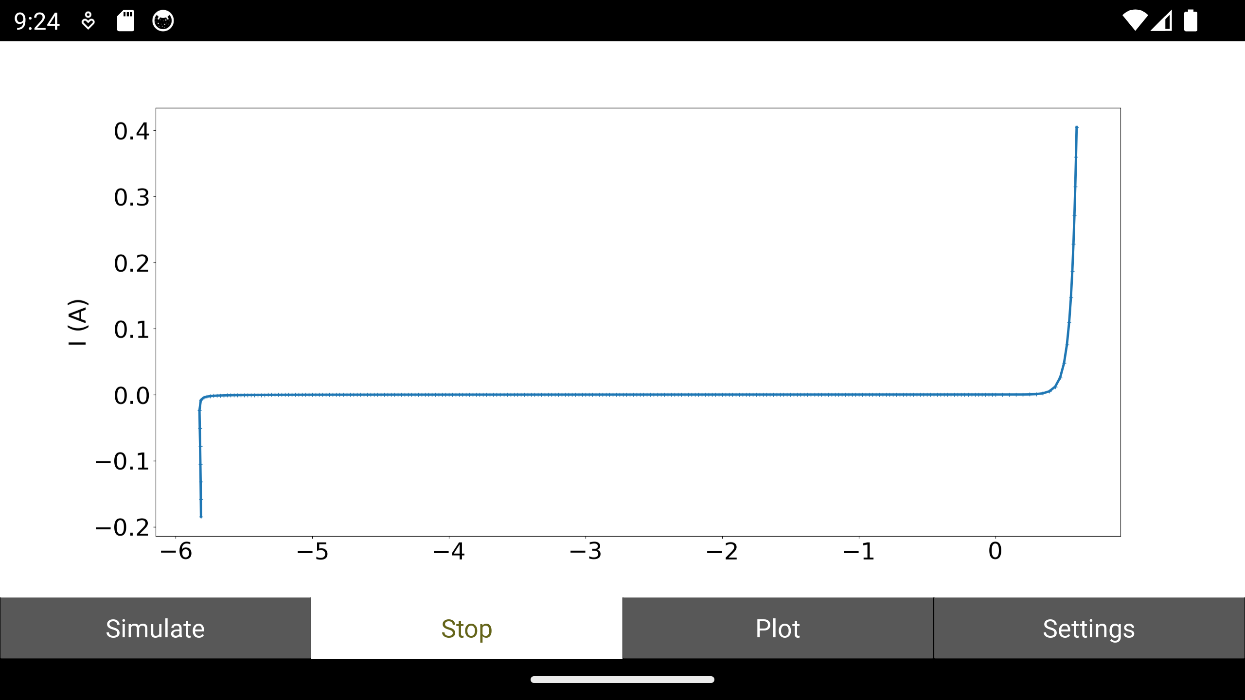
DEVSIM as TCAD mobile app

DEVSIM: TCAD mobile app


Now through January 18, 2024, the TCAD app is free for download. After this, you will be entitled to any free future updates [read more...]

  • App is renamed to “TCAD app”
  • Impact ionization model added
  • Menus updated
  • Easier plot navigation
  • Series resistance available to aid in impact ionization model results
  • Stop simulation and keep partial results to stop long-running simulation early

Get it on Google Play Download on the App Store

Oct 30, 2023

[paper] DEVSIM

Sanchez, J. E.,
DEVSIM: A TCAD Semiconductor Device Simulator
Journal of Open Source Software, 7(70), 3898, (2022).
DOI:10.21105/joss.03898

Abstract: DEVSIM is technology computer-aided design (TCAD) software for semiconductor device simulation. By solving the equations for electric fields and current flow, it simulates the electrical behavior of semiconductor devices, such as transistors. It can be used to model existing, fabricated devices for calibration purposes. It is also possible to explore novel device structures and exotic materials, reducing the number of costly and time-consuming manufacturing iterations While DEVSIM has limited capabilities for the creation of 1-D and 2-D meshes, the Pythoninterface allows the import of mesh structures from any format using a triangular representation (in 2-D) or a tetrahedral representation (in 3-D). This makes it possible for the user to utilize high quality open source meshing solutions.

FIG: 90-nm 3-D MOSFET. The polysilicon gate (2) is surrounded by oxide (5) and two nitride regions (3) and (4). The bulk region (1) has a 120nm drawn gate length. The source and drain contacts are both 50 nm underneath the nitride regions. A body contact was placed on the bottom of the 60nm silicon region. The oxide thickness is 4.9 nm and the device is 25nm thick.


Jun 14, 2023

[review] TCAD Simulations of Semiconductor Piezoresistance

Takaya Sugiura, Kazunori Matsuda*, Nobuhiko Nakano
Review: Numerical Simulations of Semiconductor Piezoresistance for Computer-Aided Designs
in IEEE J-EDS, vol. 11, pp. 325-336, 2023
DOI: 10.1109/JEDS.2023.3281866

  Department of Electronics and Electrical Engineering, Keio University, Yokohama, Kanagawa, Japan
* Division of Electrical, Electronic and Infocommunications Engineering, Osaka University, Suita, Japan

Abstract: The field of piezoresistance has mainly advanced through experimental research; however, the improved accuracy of simulations and the emergence of new materials have increased the importance of simulations in this field. This review discusses the methods and current topics related to simulations of piezoresistive devices. Advancing simulation modeling will facilitate the computer-aided design of piezoresistive devices, and this review introduces the means of establishing these models by discussing the current studies on simulations and calculations in this field. Two simulation methods currently exist namely, device simulations and first-principles theoretical analysis. This review focuses on numerical simulation approaches for modeling of the piezoresistive effect using the multiphysics simulations of the mechanical and electrical behaviors of piezoresistive materials.

FIG: Basic simulation flow for studies on semiconductor piezoresistors.

Jun 7, 2023

[paper] Teaching Traditional TCAD New Tricks

Sanghoon Myung1, Wonik Jang1, Seonghoon Jin2
Myung Choe1, Changwook Jeong1, and Dae Sin Kim1
Restructuring TCAD System:
Teaching Traditional TCAD New Tricks
DOI: 10.1109/IEDM19574.2021.9720616

1Data and Information Technology Center, Samsung Electronics.
2Device Lab, Samsung Semiconductor Inc.


Abstract : Traditional TCAD simulation has succeeded in predicting and optimizing the device performance; however, it still faces a massive challenge - a high computational cost. There have been many attempts to replace TCAD with deep learning, but it has not yet been completely replaced. This paper presents a novel algorithm restructuring the traditional TCAD system. The proposed algorithm predicts three-dimensional (3D) TCAD simulation in real-time while capturing a variance, enables deep learning and TCAD to complement each other, and fully resolves convergence errors.

Fig: (a) A TCAD process simulation result. (b) A prediction result of RTT process model.
(c) 1D doping concentration plot in the horizontal direction below the gate.
(d) 1D doping concentration plot in the vertical direction at the center of drain.


Mar 3, 2022

[paper] Charge Trapping/Detrapping in Scaled MOSFETs

Ruben Asanovski, Pierpaolo Palestri*, and Luca Selmi
Importance of Charge Trapping/Detrapping Involving the Gate Electrode on the Noise Currents of Scaled MOSFETs
IEEE TED, Vol. 69, No. 3, March 2022 1313
DOI: 10.1109/TED.2022.3147158
  
 Università degli Studi di Modena e Reggio Emilia, Modena, Italy
*Università degli Studi di Udine, Udine, Italy

Abstract: Carrier trapping/detrapping from/to the gate into dielectric traps is often neglected when modeling noise in MOSFETs and, to the best of our knowledge, no systematic study of its impacts on scaled devices is available. In this article, we show that this trapping mechanism cannot be neglected in nowadays aggressively scaled gate dielectric thicknesses without causing errors up to several orders of magnitude in the estimation of the drain current noise. The noise generation mechanism is modeled analytically and then analyzed through the use of 2-D and 3-D TCAD simulations of scaled MOSFETs with different architectures and channel/gate-stack materials. The results provide new insights for technology and device designers, highlight the relevance of the choice of the gate metal work function (WF) and the role of valence band electron trapping at high gate voltages.
Fig: (a) FinFET with the single trap location highlighted. (b) Drain current noise comparison between TCAD simulations at VGS = 0.7 V, VDS = 25 mV and single trap located as in (a).


Oct 20, 2021

[paper] Compact model of 3D NAND

Kul Lee and Hyungcheol Shin
Distinguishing capture cross section parameter between 
in GIDL erase compact model and TCAD
Japanese Journal of Applied Physics. 2021 Oct 14.
 
ISRC and School of Electrical Engineering and Computer Science, Seoul National University, (KR)
 

Abstract: Compact model of 3D NAND enables simulation at circuit- or system- level. Although compact model for gate-induced-drain-leakage(GIDL)-assisted erase has been proposed in previous study, it is difficult to be used practically because it has not been properly validated. In particular, capture-cross-section (CCS) value that is far from the real value is used. Also, it doesn’t consider the latest device structure and its operation. In this paper, conventional GIDL-assisted erase compact model is validated using TCAD and improved more practically. It is confirmed that CCS should be distinguished in TCAD and compact model due to their different definition in each of them. Based on their physical differences, equation that can interconvert them is proposed and the model is successfully validated with proper CCS. Finally, the advanced GIDL-assisted erase compact model considering tapered angle, single-side injection and word-line voltage is suggested.

Fig: Schematic cross section of 3D NAND string considering tapered angle. Double stacking and singe-side GIDL injection are assumed. It is assumed that the upper and lower stacks have the same dimension parameters.


Jul 26, 2021

[paper] NCFET CMOS Logic

Reinaldo Vega, Senior Member, IEEE, Takashi Ando*, Senior Member, IEEE,  
Timothy Philip, Member, IEEE
Junction Design and Complementary Capacitance Matching 
for NCFET CMOS Logic 
IEEE J-EDS 2021
DOI 10.1109/JEDS.2021.3095923

IBM Research, Albany, NY 12203
* IBM T.J. Watson Research Center, Yorktown Heights, NY 10598

Abstract: Negative capacitance field effect transistors (NCFETs) are modeled in this study, with an emphasis on junction design, implications of complementary logic, and device Vt menu enablement. Contrary to conventional MOSFET design, increased junction overlap is beneficial to NCFETs, provided the remnant polarization (Pr) is high enough. Combining broad junctions with complementary capacitance matching (CCM) in MFMIS (metal/ ferroelectric/ metal/ insulator/ semiconductor) NCFETs, it is shown that super-steep and non-hysteretic switching are not mutually exclusive, and that it is theoretically possible to achieve non-hysteretic sub-5 mV/dec SS over > 6 decades. In a CMOS circuit, due to CCM, low-Vt pairs provide steeper subthreshold swing (SS) than high-Vt pairs. Transient power/performance is also modeled, and it is shown that a DC optimal NCFET design, employing broad junctions, CCM, and a low-Vt NFET/PFET pair, does not translate to improved AC power/performance in unloaded circuits compared to a conventional FET reference. It is also shown that the same non-hysteretic DC design point is hysteretic in AC and may also lead to full polarization switching at higher voltages. Thus, a usable voltage window for AC NCFET operation forces a retreat from the DC-optimal design point.

Fig: Equivalent capacitance network and illustrative C-V curve showing NMOS and NC curves. CNC > CINV results in non-hysteretic switching, but low voltage gain in the off-state due to CNC >> COV. Setting CNC to CNC2, which is matched more closely to COV, results in very low SS, but also hysteretic switching as CNC2 < CINV. 

Acknowledgment: The authors would like to thank Paul Solomon and Prof. Sayeef Salahuddin for insightful discussions, as well as Synopsys for technical support.


Jun 29, 2021

[paper] Nano Device Simulator

Zlatan Stanojevic , Member, IEEE, Chen-Ming Tsai, Georg Strof, Ferdinand Mitterbauer, Oskar Baumgartner, Member, IEEE, Christian Kernstock, and Markus Karner, Member, IEEE
Nano Device Simulator - A Practical Subband-BTE Solver for Path-Finding and DTCO
in IEEE TED, Open Access, June 2021
DOI: 10.1109/TED.2021.3079884.
Global TCAD Solutions GmbH, 1010 Vienna

Abstract: We present an in-depth discussion on the subband Boltzmann transport (SBTE) methodology, its evolution, and its application to the simulation of nanoscale MOSFETs. The evolution of the method is presented from the point of view of developing a commercial general purpose SBTE solver, the GTS nano device simulator (NDS). We show a wide range of applications SBTE is suited for, including state-of-the-art nonplanar and well-established planar technologies. It is demonstrated how SBTE can be employed both as a path-finding tool and a fundamental component in a DTCO-flow. 
Fig: NDS simulation of a device generated using level-set topography simulation; left: level-set generated FinFET with complex warped surfaces, typical of topography simulation; the analytical doping is shown; middle: the SBTE domain is cut out of the device and meshed using an extruded grid, and mixed with the mesh of the rest of the device; cuts are then extracted from the SBTE domain and remeshed; right: electron drift velocity in the FinFET, DD versus SBTE; the SBTE result clearly shows the velocity overshoot effect not seen in the DD solution.

Acknowledgment: The authors would like to thank Dr. Edward Chen for many fruitful discussions and the continued valuable feedback.


May 25, 2021

[papers] Aging and Device Reliability Compact Modeling

IEEE International Reliability Physics Symposium
(IRPS 2021)

[1] N. Chatterjee, J. Ortega, I. Meric, P. Xiao and I. Tsameret, "Machine Learning On Transistor Aging Data: Test Time Reduction and Modeling for Novel Devices," 2021 IEEE International Reliability Physics Symposium (IRPS), 2021, pp. 1-9, doi: 10.1109/IRPS46558.2021.9405188.

Abstract: Accurately modeling the I-V characteristics and current degradation for transistors is central to predicting circuit end-of-life behavior. In this work, we propose a machine learning model to accurately model current degradation at various stress conditions and extend that to make nominal use-bias predictions. The model can be extended to track and predict any parametric change. We show an excellent agreement of the model with experimental results. Furthermore, we use a deep neural network to model the I-V characteristics of aged transistors over a wide drain and gate playback bias range and show an excellent agreement with experimental results. We show that the model is reliably able to interpolate and extrapolate demonstrating that it learns the underlying functional form of the data.

URL: https://ieeexplore.ieee.org/stamp/stamp.jsp?tp=&arnumber=9405188&isnumber=9405088

[2] P. B. Vyas et al., "Reliability-Conscious MOSFET Compact Modeling with Focus on the Defect-Screening Effect of Hot-Carrier Injection," 2021 IEEE International Reliability Physics Symposium (IRPS), 2021, pp. 1-4, doi: 10.1109/IRPS46558.2021.9405197.

Abstract: Accurate prediction of device aging plays a vital role in the circuit design of advanced-node CMOS technologies. In particular, hot-carrier induced aging is so complicated that its modeling is often significantly simplified, with focus limited to digital circuits. We present here a novel reliability-aware compact modeling method that can accurately capture the full post-stress I-V characteristics of the MOSFET, taking into account the impact of drain depletion region on induced defects.

URL: https://ieeexplore.ieee.org/stamp/stamp.jsp?tp=&arnumber=9405197&isnumber=9405088

[3] Z. Wu et al., "Physics-based device aging modelling framework for accurate circuit reliability assessment," 2021 IEEE International Reliability Physics Symposium (IRPS), 2021, pp. 1-6, doi: 10.1109/IRPS46558.2021.9405106.

Abstract: An analytical device aging modelling framework, ranging from microscopic degradation physics up to the aged I-V characteristics, is demonstrated. We first expand our reliability oriented I-V compact model, now including temperature and body-bias effects; second, we propose an analytical solution for channel carrier profiling which-compared to our previous work-circumvents the need of TCAD aid; third, through Poisson's equation, we convert the extracted carrier density profile into channel lateral and oxide electric fields; fourth, we represent the device as an equivalent ballistic MOSFETs chain to enable channel “slicing” and propagate local degradation into the aged I-V characteristics, without requiring computationally-intensive self-consistent calculations. The local degradation in each channel “slice” is calculated with physics-based reliability models (2-state NMP, SVE/MVE). The demonstrated aging modelling framework is verified against TCAD and validated across a broad range of VG/VD/T stress conditions in a scaled finFET technology.

URL: https://ieeexplore.ieee.org/stamp/stamp.jsp?tp=&arnumber=9405106&isnumber=9405088

Mar 7, 2021

[C4P] SISPAD 2021, September 27-29

International Conference on Simulation of Semiconductor Processes and Devices
SISPAD 2021, September 27-29
The abstract submission deadline April 9th.

Two-page abstract (text and figures, A4, 10 – 12 pt, pdf) should be sent to <sispad2021@utdallas.edu>  Authors of accepted papers are requested to submit a four-page final paper which will be published in the conference proceedings. The deadline for submission of the four-page final paper is July 9, 2021.

The SISPAD conference series provides an open forum for the presentation of the latest results and trends in process and device simulation. The conference is the leading forum for Technology Computer-Aided Design (TCAD) and is held alternatingly in the United States, Japan, and Europe in September.

Original contributions are solicited for SISPAD 2021 on topics that include but are not limited to:
  • Modeling and simulation of established semiconductor device, including FinFETs, GAA FETs, ultra-thin SOI devices, optoelectronic devices, TFTs, sensors, power electronic devices, and organic electronic devices.
  • Modeling and simulation of emerging devices including tunnel FETs, SETs, spintronic devices, straintronic devices, bio-electronic devices, and new material-based devices for various applications
  • Modeling and simulation of interconnects, including noise and parasitic effects
  • Modeling and simulation of all sorts of semiconductor processes, including first principles material design, and growth simulation of nano-scale fabrication
  • Advances in fundamental aspects of device modeling and simulation, including of charge, spin, and thermal transport, of collective states including spin/magnetic and charge, and of fluctuation, noise, and reliability.
  • Numerical methods and algorithms, including grid generation, user-interface, and visualization
  • Compact modeling for circuit simulation, including low-power, high frequency, and power electronics applications
  • Process/device/circuit co-simulation in context with system design and verification, including for emerging devices
  • Modeling and simulation of equipment, topography, lithography
  • Benchmarking, calibration, and verification of simulators

Mar 1, 2021

[papers] compact/SPICE modeling

[1] M. Müller, P. Dollfus and M. Schröter, "1-D Drift-Diffusion Simulation of Two-Valley Semiconductors and Devices," in IEEE Transactions on Electron Devices, vol. 68, no. 3, pp. 1221-1227, March 2021, doi: 10.1109/TED.2021.3051552.

Abstract: A two-valley formulation of 1-D drift-diffusion transport is presented that takes the coupling between the valleys into account via a new approximation for the nonlocal electric field. The proposed formulation is suitable for the simulation of III–V heterojunction bipolar transistors as opposed to formulations that employ the single electron gas approximation with a modified velocity-field model, which also causes convergence problems. Based on Boltzmann transport equation simulations, model parameters of the proposed two-valley formulation are given for GaAs, InP, InAs, and GaSb at room temperature. Applications of the new formulation are also demonstrated. 
Code/Dataset: This article contains datasets made available via IEEE DataPort, a repository of datasets intended to facilitate analysis and enable reproducible research. Click the dataset name below to access it on the IEEE DataPort website.

[2] A. Rawat et al., "Experimental Validation of Process-Induced Variability Aware SPICE Simulation Platform for Sub-20 nm FinFET Technologies," in IEEE Transactions on Electron Devices, vol. 68, no. 3, pp. 976-980, March 2021, doi: 10.1109/TED.2021.3053185.

Abstract:We propose an experimentally validated physics-based process-induced variability (PIV) aware SPICE simulation framework–enabling the estimation of performance variation due to line-edge-roughness (LER), metal-gate-granularity (MGG), random-dopant-fluctuation (RDF), and oxide-thickness-variation (OTV) at sub-20 nm technology node devices. The framework utilizes LER, RDF, OTV, and MGG defining parameters such as fin-edge correlation coefficient (ρ), autocorrelation length (Λ), grain-size (GS), σ[EOT], etc. as the inputs, and produces IdVg distribution of ensemble size 250 as an output. We have validated the framework against 14 nm FinFET experimental data for IdVg trends as well as for the threshold-voltage (Vth), ON-current (Ion), and subthreshold slope (SS) distributions for a range of device dimensions with a reasonably good match. The worst and the best case R square errors are 0.64 and 0.98, respectively, for the validation. The very nature of the proposed framework allows the designers to use it for a vast range of process technologies. Such models are of dual importance, as it enables a PIV aware prediction of circuit-level performance, and provides a platform to estimate PIV parameters efficiently, on-par with sophisticated structural characterization tools.

[3] Blake W. Nelson, Andrew N. Lemmon, Sergio J. Jimenez, H. Alan Mantooth, Brian T. DeBoi, Christopher D. New, Md Maksudul Hossain, "Computational Efficiency Analysis of SiC MOSFET Models in SPICE: Dynamic Behavior," in IEEE Open Journal of Power Electronics, vol. 2, pp. 106-123, 2021, doi: 10.1109/OJPEL.2021.3056075.

Abstract: Transient simulation of complex converter topologies is a challenging problem, especially in detailed analysis tools like SPICE. Transistor models presented for SPICE are often evaluated by accuracy, with less consideration for the computational cost of model elements. In order to optimize models for application simulations, this research quantifies the relative simulation performance of modeling approaches and contextualizes the results with regard to accuracy. It is well established that the primary contributor to semiconductor dynamic behavior is the voltage-dependent interelectrode capacitances. Therefore, this study isolates these model components to resolve their influence on model accuracy and run-time. Both the voltage-dependencies modeled, and the mathematic formulation chosen strongly influence the accuracy of interelectrode capacitance models. In addition to these factors, the specific implementation chosen within SPICE also determines simulation performance. Through careful evaluation of these factors, this study offers specific recommendations for optimal implementations of interelectrode capacitances in SPICE.
Fig: DPT system schematic, components, and metrology.

[4] Sherif M. Sharroush & Yasser S. Abdalla; Parameter extraction and modelling of the MOS transistor by an equivalent resistance, Mathematical and Computer Modelling of Dynamical Systems, (2021) 27:1, 50-86, DOI: 10.1080/13873954.2020.1857790

Abstract: During the analysis of multi-transistor circuits, the need arises to evaluate the time delay or the power consumption of the circuit. Due to the complexity of the transistor model, several complicated equations arise from which a compact-form solution cannot be obtained and a suitable physical insight cannot be drawn. With this regard, two contributions are presented in this paper. The first one is a fully analytical parameter extraction approach to be applied on the MOS transistors. The second one is a quantitative method for simplifying the analysis of MOS circuits by modelling the MOS transistor by a suitable equivalent resistance adopting the time-delay or the power-consumption equivalence criteria. The parameter-extraction method is verified by using the extracted parameters in the derived expressions according to the second contribution. Compared to other representations, the agreement of the proposed model with the simulation results is very good.
Fig: Finding Vthn0 as the intercept of the linear portion of the Id-Vgs characteristics with the horizontal axis. The curve corresponds to Vds=1V. The term ‘exact relationship’ means data from the simulation results




Feb 26, 2021

[DAY 2] 1st Asia/South Pacific MOS-AK Workshop

Arbeitskreis Modellierung von Systemen und Parameterextraktion
Modeling of Systems and Parameter Extraction Working Group
1st Asia/South Pacific MOS-AK Workshop
(virtual/online) FEB. 25-26, 2021

Day2: FEB.26
Session C Chair: Sadayuki Yoshitomi, Kioxia (J)

[8] eSim: An open source CAD software for circuit simulation
Kannan Moudgalya
IIT Bombay (IN)

[9] A modular approach to next generation Qucs
Felix Salfelder and Mike Brinson
QUCS Team; Centre for Communications Technology, London Metropolitan University (UK)

[12] Machine learning-based approach to model and analyze GaN power devices
Tian-Li Wu
National Yang Ming Chiao Tung University, Taiwan (TW)

[11] TCAD-inspired compact modeling approach
Sung-Min Hong and Kwang-Woon Lee
Gwangju GIST (KR)

Session D Chair: Sheikh Aamir Ahsan, NIT Srinagar (IN)
[10] An Innovative Technique for Ultrafast Carrier Dynamics and THz Conductivities of Semiconductor Nanomaterials
Praveen Kr. Saxena and Fanish Kr. Gupta
Tech Next Lab, Lucknow (IN)

[13] Compact Modeling of 3D NAND Flash Memory for Diverse Unconventional Analog Applications
Shubham Sahay
IIT Kanpur (IN)

[14] Steep Subthreshold Slope PN-Body Tied SOI-FET for Ultralow Power LSI, Sensor, and Neuromorphic Chip
Takayuki Mori and Jiro Ida
Kanazawa Institute of Technology, Nonoichi (J)

[Pic] Group photo of selected MOS-AK participants attending 2nd Day of the workshop


[DAY 1] 1st Asia/South Pacific MOS-AK Workshop

Arbeitskreis Modellierung von Systemen und Parameterextraktion
Modeling of Systems and Parameter Extraction Working Group
1st Asia/South Pacific MOS-AK Workshop
(virtual/online) FEB. 25-26, 2021

DAY 1: FEB. 25, 2021
Session A Chair: Usha Gogineni, ams AG, Hyderabad (IN)

[1] New Insights in Low Frequency Noise Characteristics in PE-BJTs
Peijian Zhang and Ma Long
Science and Technology on Analog Integrated Circuit Laboratory; WHU (CN), Keysight Technologies (US)

[2] Direct white noise characterization of short-channel MOSFETs
K. Ohmori and S. Amakawa
DeviceLab, Tsukuba (J)

[3] SPICE Modeling of 2D-material based FETs with Schottky-barrier contacts
Sheikh Aamir Ahsan
Nanoelectronics Research and Development Group, NIT Srinagar, Jammu and Kashmir (IN)


[4] Physics-based model of SiC MOSFETs including high voltage and current regions
Sourabh Khandelwal, Cristino Salcines, and Ingmar Kallfass
Macquarie University Sydney (AU), University of Stuttgart (D)

Session B Chair: Daniel Tomaszewski, IMiF, Warszaw (PL)
[5] Compact Modeling for Gate-All-Around FET Technology
Avirup Dasgupta
IIT Roorkee (IN)


[6] BSIM-HV: Advanced High Voltage MOSFET Compact Model
Harshit Agarwal
IIT Jodhpur (IN)

[7] ASCENT+ Transnational Access for the nanoelectronics
Georgios Fagas
Tyndall (IE)

[Pic] Group photo of selected MOS-AK participants attending 1st Day of the workshop

Jan 8, 2021

[C4P] New simulation methodologies for next-generation TCAD

Call for Papers for a Special Issue of
IEEE Transactions on Electron Devices on
"New simulation methodologies for next-generation TCAD" 
Submission deadline: February 28, 2021 
Publication date: November 2021

Technology Computer Aided Design is used to simulate semiconductor processes and devices,a field which has become increasingly complex and heterogeneous. Processing of integrated circuits requires nowadays over 400 process steps, and the resultant devices often have a complicated 3D structure and contain various materials. The full device behavior can only be understood by considering effects on all length scales from atomistic (interfaces, defects etc.) over nanometric (quantum confinement, non-bulk properties etc.) to full chip dimensions (strain, heat transport etc.), and time scales from femtoseconds to seconds. Voltages, currents and charges have been scaled to such low levels that electronic noise, statistical effects and process variations have a strong impact. Devices based on new materials (e.g. 2D crystals) and physical principles (ferroelectrics, magnetic materials, qubits etc.) challenge standard TCAD approaches. While the simulation methods developed by the physics community can describe the basic device behavior, they often lack important simulation capabilities like, for example, transient simulations or integration with other TCAD tools and are too slow for daily use. Due to the complexity of semiconductor technology, it becomes more and more difficult to assess the impact of a change in processing or device structure on circuit performance by looking at a single aspect of an isolated device under idealized conditions. Instead a TCAD tool chain is required that can handle realistic device structures embedded in a chip environment. New methodologies are required for all aspects of TCAD to ensure an efficient tool chain covering from atomistic effects to circuit behavior based on flexible simulation models that can handle new materials, device principles and the ensuing large-scale simulations.
This Special Issue of the IEEE Transactions on Electron Devices will feature the most recent developments and the state of the art in the field of TCAD for processing and for device behavior with a focus on new methodologies that improve the tool chain. Papers must be new and present original material that has not been copyrighted, published or accepted for publications in any other archival publications, that is not currently being considered for publications elsewhere, and that will not be submitted elsewhere while under considerations by the Transactions on Electron Devices.

Topics of interest include, but are not limited to:
• Artificial Intelligence applied to TCAD
• TCAD device models for
• new materials (2D materials, oxides, organic semiconductors, oxide semiconductors,
nanowire devices etc.)
• new device types (magnetic devices, memristors, spintronics, qubits, sensors etc.)
• physical effects (ferroelectric dielectrics, thermal transport at nanoscale, atomistic
simulation etc.)
• simulation conditions that push the limits of standard TCAD: ballistic transport, THz
frequencies, cryogenic conditions, device degradation, electromagnetic and plasma
waves in active devices, transient simulations, noise and fluctuations, microscopic 
simulation of large power devices
• Process simulation
• Atomistic process simulation to generate structures for atomistic device simulations
(including both interconnects and transistors)
• Gate stack modeling including dipole diffusion
• Stress simulation for nanosheet and forksheet devices and stress simulations
including layout effects
• Topological simulation
• Equipment simulation
• New methods for the TCAD tool chain
• Self-consistent integration of simulation models into the hierarchy
• Device-circuit interaction
• Multi-physics and multi-scale integration
• Efficient use of the data produced along the chain
• Workflow improvements
• Methods that improve the turn-around-time for TCAD simulations

Submission instructions: Manuscripts should be submitted in a double column format
using an IEEE style file. Please visit the following link to download the templates:
http://www.ieee.org/publications_standards/publications/authors/author_templates.html
In your cover letter, please indicate that your submission is for this special issue.

Guest Editors:
1. Prof. Fabrizio Bonani, Politecnico di Torino, Italy
2. Dr. Stephen Cea, Intel Corp., USA
3. Prof. Elena Gnani, University of Bologna, Italy
4. Prof. Sung-Min Hong, GIST, Republic of Korea
5. Dr. Seonghoon Jin, Samsung, USA
6. Prof. Christoph Jungemann, RWTH Aachen, Germany
7. Prof. Xiaoyan Liu, Peking University, China
8. Dr. Victor Moroz, Synopsys, USA
9. Dr. Anne Verhulst, imec, Belgium

Jan 5, 2021

[paper] NESS Open-Source TCAD Environment

Cristina Medina-Bailon, Tapas Dutta, Fikru Adamu-Lema, Ali Rezaei, Daniel Nagy,
Vihar P. Georgiev, and Asen Asenov
Nano-Electronic Simulation Software (NESS): 
A Novel Open-Source TCAD Simulation Environment
Journal of Microelectronic Manufacturing
Vol 3 (4) : 20030407 2020
DOI:  10.33079/jomm.20030407

Abstract: This paper presents the latest status of the open source advanced TCAD simulator called Nano-Electronic Simulation Software (NESS) which is currently under development at the Device Modeling Group of the University of Glasgow. NESS is designed with the main aim to provide an open, flexible, and easy to use simulation environment where users are able not only to perform numerical simulations but also to develop and implement new simulation methods and models. Currently, NESS is organized into two main components: the structure generator and a collection of different numerical solvers; which are linked to supporting components such as an effective mass extractor and materials database. This paper gives a brief overview of each of the components by describing their main capabilities, structure, and theory behind each one of them. Moreover, to illustrate the capabilities of each component, here we have given examples considering various device structures, architectures, materials, etc. at multiple simulation conditions. We expect that NESS will prove to be a great tool for both conventional as well as exploratory device research programs and projects.
Fig: Randomly generated atomistic device considering random discrete dopants (RDD) and metal gate granularity (MGG) in the NESS simulation domain

Acknowledgments: This project was initiated by the European Union Horizon 2020 research and innovation programme under grant agreement No. 688101 SUPERAID7 and has received further funding from EPSRC UKRI Innovation Fellowship scheme under grant agreement No. EP/S001131/1 (QSEE), No. EP/P009972/1 (QUANTDEVMOD) and No. EP/S000259/1 (Variability PDK for design based research on FPGA/neuro computing); and from H2020-FETOPEN-2019 scheme under grant agreement No.862539-Electromed-FET OPEN. The coauthors would like to thank Dr. Carrillo-Nuñez, Dr. Lee, Dr. Berrada, Dr. Badami, and Dr. Duan for their former contribution to NESS; as well as Dr. Donetti for the possibility of using the 1DMC tool. 

Nov 19, 2020

[paper] HEMT RF/Analog Performance

M. Khaouani1,H. Bencherif2, A. Hamdoune1, A. Belarbi3, Z. Kourdi4
RF/analog Performance Assessment of High Frequency, Low Power In0.3Al0.7As/InAs/InSb/In0.3Al0.7As HEMT Under High Temperature Effect
Transactions on Electrical and Electronic Materials
The Korean Institute of Electrical and Electronic Material Engineers 2020
DOI: 10.1007/s42341-020-00250-8

1 Department of Genie Electric and Electronics, Unit Research of Material and Renewable Energies, University Aboubek Belkaid, Tlemcen, Algeria
2 LAAAS Laboratory, University of Batna 2, Batna, Algeria
3 Center Exploitation Telecommunication Satellite– Bouchaoui-Alger, Algeria Space Agency, Algiers, Algeria
4 Center Exploitation Telecommunication Satellite– Oran-Alger, Algeria Space Agency, Algiers, Algeria


In0.3Al0.7As/InAs/InSb/In0.3Al0.7As In this paper, we performed a Pseudo-morphic High Electron Mobility Transistors (pHEMT) In0.3Al0.7As/InAs/InSb/In0.3Al0.7As using commercial TCAD. RF and analog electrical characteristics are assessed under high temperature effect. The impact of the temperature is evaluated referring to a device at room temperature. In particular, the threshold voltage (Vth), transconductance (gm), and Ion/Ioff ratio are calculated in the temperature range of 300K to 700K. The primary device exhibits a drain current of 950mA, a Vth of -1.75V, a high value of gm of 650 mS/mm, Ion/Ioff ratio of 1E6, a transition frequency (fT) of 790GHz, and a maximum frequency (fmax) of 1.4THz. The achieved results show that increasing temperature act to decrease current, reduce gm, and Ion/Ioff ratio. In more detail high temperature causes a phonon scattering mechanism happening that determine in turn a reduced drain current and shift positively the threshold voltage resulting in hindering the device DC/AC capability. 
Fig: 2D cross section of In0.3Al0.7As/InAs/InSb/In0.3Al0.7AsAs PHEMT


Nov 3, 2020

Congratulations to Prof. Robert W. Dutton

The 2020 IEEE EDS Celebrated Member and Esteemed EDS Alumni


Dr. Dutton received his degrees from the University of California, Berkeley, and currently instructs electrical engineering at Stanford University. Current members of EDS take pride in the Celebrated Members' accomplishments, drawing from their achievements as inspiration to advance and achieve success in various fields. The award presentation will be held virtually during the 2020 IEDM in December [read more...]

ROBERT W. DUTTON
Robert W. Dutton received the B.S., M.S., and Ph.D. in Electrical Engineering degrees from the University of California, Berkeley, in 1966, 1967, and 1970, respectively. 
He is currently Robert and Barbara Kleist Professor of Electrical Engineering at Stanford University, and Associate Chair for Undergraduate Education. He has held summer staff positions at Fairchild, Bell Telephone Laboratories, Hewlett‐Packard, IBM Research, and Matsushita during 1967, 1973, 1975, 1977, and 1988 respectively. His research interests focus on integrated circuit process, device, and circuit technologies, especially the use of computer‐aided design (CAD) and parallel computational methods. He has published more than 200 journal articles and graduated more than four dozen doctorate students. 
Dr. Dutton was Editor of the IEEE Transactions on Computer Aided Design from 1984 to 1986, the winner of the 1987 IEEE J. J. Ebers Award, 1988 Guggenheim Fellowship to study in Japan, elected to the National Academy of Engineering in 1991, 1996 Jack A. Morton Award, 2000 C&C Prize Japan, University Researcher Award, Semiconductor Industry Association (2000), Phil Kaufman Award, Electronic Design Automation Consortium (2006), and 2014 Bass University Fellow in Undergraduate Education Program, Stanford University.

Oct 9, 2020

[paper] TCAD-Machine Learning Framework

Hiu Yung Wong1 (Senior Member, IEEE), Ming Xiao2, Boyan Wang2, Yan Ka Chiu1, Xiaodong Yan3, Jiahui Ma3, Kohei Sasaki4, Han Wang3 (Senior Member, IEEE)
and Yuhao Zhang2 (Member, IEEE)
TCAD-Machine Learning Framework for Device Variation and Operating Temperature Analysis with Experimental Demonstration
IEEE J-EDS, vol. 8, pp. 992-1000, 2020
doi: 10.1109/JEDS.2020.3024669.

1Department of Electrical Engineering, San Jose State University, San Jose, CA 95112, USA
2Virginia Polytechnic Institute, State University, Blacksburg, VA 24060, USA
3Ming Hsieh Department of Electrical Engineering, University of Southern California, Los Angeles, CA 90089, USA
4Development Department, Novel Crystal Technology Inc., Sayama 3501328, Japan

Abstract: This work, for the first time, experimentally demonstrates a TCAD-Machine Learning (TCADML) framework to assist the analysis of device-to-device variation and operating (ambient) temperature without the need of physical quantities extraction. The ML algorithm used in this work is the Principal Component Analysis (PCA) followed by third order polynomial regression. After calibrated to limited ‘expensive’ experimental data, ‘low cost’ TCAD simulation is used to generate a large amount of device data to train the ML model. The ML was then used to identify the root cause of device variation and operating temperature from any given experimental current-voltage (I-V) characteristics. We applied this framework to study the ultra-wide-bandgap gallium oxide (Ga2O3) Schottky barrier diode (SBD), an emerging device technology that holds great promise for temperature sensing, RF, and power applications in harsh environments. After calibration, over 150,000 electrothermal TCAD simulations are performed with random variation of physical parameters (anode effective work function, drift layer doping, and drift layer thickness) and operating temperature. An ML model is trained using these TCAD data and we found 1,000-10,000 TCAD data can train an accurate machine. We show that without physical quantities extraction, performing PCA is essential for the TCAD trained ML model to be applicable to analyze experimental characteristics. The physical parameters and temperatures predicted by the ML model show good agreement with experimental analysis. Our TCAD-ML framework shows great promise to accelerate the development of new device technologies with a significantly more efficient process of material and device experimentation.


FIG: Flow chart diagram of the proposed TCAD-Machine Learning framework. All components are demonstrated in this article except the MLDatabase which stores previously trained ML algorithms.

Acknowledgment: The authors thank Dr. Pooya Jannaty of Cruise and Dr. Philip Leong of the University of Sydney for the discussion of ML algorithms. The experimental work is in part supported by the Southeastern Center for Electrical Engineering Education program and the High Density Integration industry mini-consortium of the Center for Power Electronics Systems at Virginia Tech.


Sep 21, 2020

[tutorial] next generation 3D nano device simulator

Single-electron transistor - laterally defined quantum dot - 3D Tutorial
Stefan Birner
https://www.nextnano.com

Single-electron transistor - laterally defined quantum dot In this tutorial, we simulate an AlGaAs/GaAs heterostructure grown along the z direction. This structure leads to a two-dimensional electron gas (2DEG). By appying a gate voltage on top of the structure in the (x,y) plane, one is able to deplete the 2DEG and a laterally defined QD is formed. By adjusting the gate voltage, one is able to tune the number of electrons that are inside the QD.
This figure shows the conduction band edge Ec(x,y) and the electron density n(x,y) for the 2DEG plane, i.e. at z = 8 nm below the GaAs/AlGaAs heterojuntion. The geometry of the top gates is indicated by the blue regions. The following figure shows the calculated conduction band edge and the electron density of the heterostructure. The results are similar to Fig. 4 in paper [1].
The following figure shows two 2D slices through the lateral (x,y) plane at a distance of 8 nm below the AlGaAs/GaAs interface. In the middle, the electron density is shown. The electron density has been calculated classically. At the bottom, the conduction band edge is shown. The results are similar to Fig. 5 in paper [1]. At the top, the four gates are shown.

REF:
[1] A. Scholze, A. Schenk, W. Fichtner; Single-Electron Device Simulation; IEEE TED 47, 1811 (2000)