Showing posts with label 3D. Show all posts

Nov 2, 2023

[workshop] FreeCAD 3D parametric modeler

PSG COLLEGE OF TECHNOLOGY, COIMBATORE
9 DECEMBER, 2023

About the FreeCAD
FreeCAD is a general purpose open source parametric 3D CAD modeller. FreeCAD is aimed directly at mechanical engineering and product design but, being very generic, also fits in a wider range of uses around engineering, such as architecture, finite element analysis, 3D printing, and other tasks. FreeCAD offers tools to produce, export and edit solid, full-precision models, export them for 3D printing or CNC machining, create 2D drawings and views of your models, perform analyses such as Finite Element Analyses, or export model data such as quantities or bills of materials. FreeCAD features tools similar to other popular CAD packages and therefore also falls into the category of CAD, PLM, CAx, CAE and BIM. It is a feature based parametric modeler with a modular software architecture, making it possible to provide additional functionality without modifying the core system. As with other CAD modelers, it has many 2D components in order to sketch planar shapes or create production drawings. FreeCAD is also fundamentally a social project, as it is developed and maintained by a community of developers and users united by their passion for FreeCAD. In precise FreeCAD is:
  • Made to build for the real world
  • A powerful solid-based geometry kernel
  • A wi(l)dly parametric environment
  • File formats frenzy
  • A parametric constraints-based 2D sketcher
  • A large (and growing) multi-specialty ecosystem
About the Workshop 
The workshop will be conducted through spoken tutorial videos of 10 minutes duration. After the workshop, a link for the video tutorials will be shared to the participants for further learning. As it is an open source software, FreeCAD can be used free of cost for educational and industrial design purposes. Participants of this workshop can install this software on their laptop during this workshop and take it with them. Target participants of this workshop include: practicing engineers, faculty members, research scholars and students.

Registration details
The registration fee for the participants (Inclusive of GST) :
  • Faculty members / Students / Research Scholars : Rs. 900/-
  • Industry participants : Rs.1200/-
No TA/ DA/ ACCOMMODATION will be provided. Payment of registration fee for the workshop can be made through online mode

https://forms.gle/xqcQLSTnJcYLK2DNA

Last date for registration: November 25, 2023

For any queries, contact
The Organizing Secretaries,
FreeCAD Workshop, PSG College of Technology,
Peelamedu, Coimbatore-641004
email : vsk.amcs@psgtech.ac.in / mrp.prod@psgtech.ac.in
Mobile : 9952418357


Sep 26, 2023

Palace: 3D Finite Element Solver for Computational Electromagnetics


Palace, for PArallel LArge-scale Computational Electromagnetics, is an open-source, parallel finite element code for full-wave 3D electromagnetic simulations in the frequency or time domain, using the MFEM finite element discretization library.

Key features:
  • Eigenmode calculations with optional material or radiative loss including lumped impedance boundaries. Automatic postprocessing of energy-participation ratios (EPRs) for circuit quantization and interface or bulk participation ratios for predicting dielectric loss.
  • Frequency domain driven simulations with surface current excitation and lumped or numeric wave port boundaries. Wideband frequency response calculation using uniform frequency space sampling or an adaptive fast frequency sweep algorithm.
  • Explicit or fully-implicit time domain solver for transient electromagnetic analysis.
  • Lumped capacitance and inductance matrix extraction via electrostatic and magnetostatic problem formulations.
  • Support for a wide range of mesh file formats for structured and unstructured meshes, with built-in uniform or region-based parallel mesh refinement.
  • Arbitrary high-order finite element spaces and curvilinear mesh support thanks to the MFEM library.
  • Scalable algorithms for the solution of linear systems of equations, including geometric multigrid (GMG), parallel sparse direct solvers, and algebraic multigrid (AMG) preconditioners, for fast performance on platforms ranging from laptops to HPC systems.
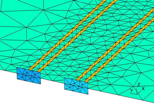
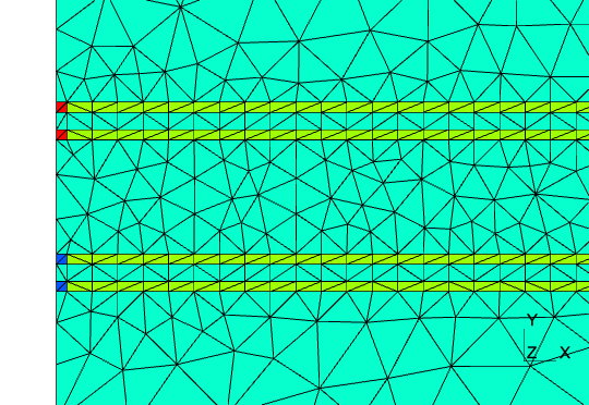
Crosstalk Between Coplanar Waveguides Example: Views of the mesh boundaries for these two configurations are shown below. In both cases the computational domain is discretized using an unstructured tetrahedral mesh. 


Jun 7, 2023

[paper] Teaching Traditional TCAD New Tricks

Sanghoon Myung1, Wonik Jang1, Seonghoon Jin2
Myung Choe1, Changwook Jeong1, and Dae Sin Kim1
Restructuring TCAD System:
Teaching Traditional TCAD New Tricks
DOI: 10.1109/IEDM19574.2021.9720616

1Data and Information Technology Center, Samsung Electronics.
2Device Lab, Samsung Semiconductor Inc.


Abstract : Traditional TCAD simulation has succeeded in predicting and optimizing the device performance; however, it still faces a massive challenge - a high computational cost. There have been many attempts to replace TCAD with deep learning, but it has not yet been completely replaced. This paper presents a novel algorithm restructuring the traditional TCAD system. The proposed algorithm predicts three-dimensional (3D) TCAD simulation in real-time while capturing a variance, enables deep learning and TCAD to complement each other, and fully resolves convergence errors.

Fig: (a) A TCAD process simulation result. (b) A prediction result of RTT process model.
(c) 1D doping concentration plot in the horizontal direction below the gate.
(d) 1D doping concentration plot in the vertical direction at the center of drain.


Feb 2, 2022

[EZMod3D] Comparing inductance extraction to measurement

EZMod3D is a division of EASii IC, which develops a 3D multi-domain physical simulation software solution (also called 3D field solver) mainly developed to process the design of integrated circuits (ASICs), printed circuit boards (PCBs) and both at the same time (CoDesign). EZMod3D was developed on the basis of an innovative solver enabling a fast simulation. This technology has allowed intensive use internally at EASii IC, targeting the requirements of R&D project: reducing iterations between design and manufacturing.

Very simple, you just need to start with your input data
  • GDS2 file, OASIS database, LEF / DEF (ASIC) or Gerber (PCB) or DXF (Packaging)
  • Technological file or materials description
  • The position of the potentials or flows to be applied
  • In pre-sizing step, you can sketchup using advanced user intergrated matrial library
FIG: An inductor, its 3D EZMod3D simulation and LCR measurements. EZMod3D now extracts inductance values and shows good agreement with measurements.
Measured value is 477nH; close to the simulated 481nH)

Oct 20, 2021

[paper] Compact model of 3D NAND

Kul Lee and Hyungcheol Shin
Distinguishing capture cross section parameter between 
in GIDL erase compact model and TCAD
Japanese Journal of Applied Physics. 2021 Oct 14.
 
ISRC and School of Electrical Engineering and Computer Science, Seoul National University, (KR)
 

Abstract: Compact model of 3D NAND enables simulation at circuit- or system- level. Although compact model for gate-induced-drain-leakage(GIDL)-assisted erase has been proposed in previous study, it is difficult to be used practically because it has not been properly validated. In particular, capture-cross-section (CCS) value that is far from the real value is used. Also, it doesn’t consider the latest device structure and its operation. In this paper, conventional GIDL-assisted erase compact model is validated using TCAD and improved more practically. It is confirmed that CCS should be distinguished in TCAD and compact model due to their different definition in each of them. Based on their physical differences, equation that can interconvert them is proposed and the model is successfully validated with proper CCS. Finally, the advanced GIDL-assisted erase compact model considering tapered angle, single-side injection and word-line voltage is suggested.

Fig: Schematic cross section of 3D NAND string considering tapered angle. Double stacking and singe-side GIDL injection are assumed. It is assumed that the upper and lower stacks have the same dimension parameters.


Mar 15, 2021

[paper] 3D integrated GaN/RF-SOI SPST switch

Frédéric Drillet, Jérôme Loraine, Hassan Saleh, Imene Lahbib, Brice Grandchamp, Lucas Iogna-Prat, Insaf Lahbib, Ousmane Sow, Albert Kumar and Gregory U'Ren 
RF Small and large signal characterization of a 3D integrated GaN/RF-SOI SPST switch 
International Journal of Microwave and Wireless Technologies, pp. 1–6, 2021.

*X-FAB France, Corbeil-Essonnes (F)

Abstract: This paper presents the radio frequency (RF) measurements of an SPST switch realized in gallium nitride (GaN)/RF-SOI technology compared to its GaN/silicon (Si) equivalent. The samples are built with an innovative 3D heterogeneous integration technique. The RF switch transistors are GaN-based and the substrate is RF-SOI. The insertion loss obtained is below 0.4 dB up to 30 GHz while being 1 dB lower than its GaN/Si equivalent. This difference comes from the vertical capacitive coupling reduction of the transistor to the substrate. This reduction is estimated to 59% based on a RC network model fitted to S-parameters measurements. In large signal, the linearity study of the substrate through coplanar waveguide transmission line characterization shows the reduction of the average power level of H2 and H3 of 30 dB up to 38 dBm of input power. The large signal characterization of the SPST shows no compression up to 38 dBm and the H2 and H3 rejection levels at 38 dBm are respectively, 68 and 75 dBc.

Fig: X-FAB 3D integration proposal cross-section (left) and the picture of a GaN coupon (right).

Acknowledgement: We would like to acknowledge the Nano2022 program for partially funding this work.

Supplementary material: The supplementary material for this article can be found at DOI: 0.101/1759078721000076

Nov 9, 2013

LETI Devices Workshop

The Churchill Hotel - 1914 Connecticut Ave. NW (across from the Hilton)
Washington D.C. 6-9 p.m on December 8, 2013

Inventing the future together: a stimulating discussion of our vision for silicon nanotechnologies in the next 10 years followed by a networking cocktail. Program is as follow:
  • Introduction (10min)
    Jean-René Lequepeys; VP Silicon Components Division 
  • Lithography cost-effective solutions for 1X nodes (15min)
    Serge Tedesco; Lithography Program Manager 
  • 3D: Dream and reality (15 min)
    Mark Scannell; Senior Business Development Manager 
  • High-performance and reliable resistive memories embedded in advanced logic CMOS technologies (15min)
    Barbara de Salvo; Advanced Memories Fellow
  • M&NEMS platforms: an enabler for the next generation of sensors in consumer electronics (15min)
    Hugues Metras; VP Strategic Partnerships, North America
  • CMOS technologies: our most power efficient solution today and our vision toward 10nm node and beyond (15 min)
    Maud Vinet; Advanced CMOS Manager
[read more...]